232 www.xilinx.com Virtex-6 FPGA GTX Transceivers User Guide
UG366 (v2.5) January 17, 2011
Chapter 4: Receiver
the CDR to be adjusted so that there is no significant phase difference between XCLK and
RXUSRCLK.
Note:
Bypassing the RX buffer is an advanced feature. RX buffer bypass can operate only under
certain system-level conditions.
To ensure that the RXRECCLK output port operates at the desired frequency in RX buffer
bypass mode, all of these conditions must be met:
• Receiver reference clock must always be toggling
• RXPOWERDOWN[0] and RXPOWERDOWN[1] must be tied Low
• RXPLLPOWERDOWN must be tied Low
• GTXRXRESET and PLLRXRESET must not be tied High
For transceivers that are not instantiated in the user design, the ISE software, version 12.1
or later, automatically ensures that the RXRECCLK performance is preserved for future
use. MGTAVCC must be supplied to these transceivers. Refer to Managing Unused GTX
Transceivers, page 276 for more information.
Ports and Attributes
Table 4-40 defines the RX buffer bypass ports.
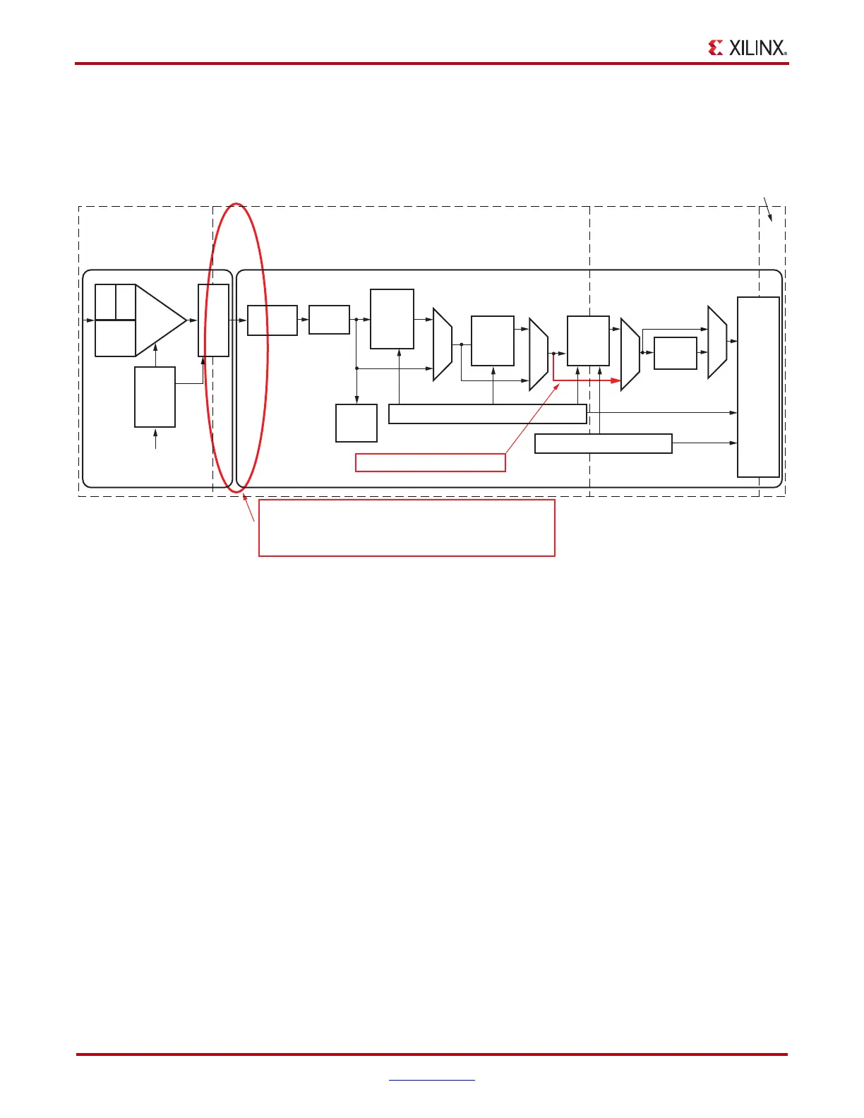
X-Ref Target - Figure 4-31
Figure 4-31: Using Phase Alignment
UG366_c4_28_051509
After phase alignment:
- SIPO parallel clock phase matches RXUSRCLK phase
- No phase difference between XCLK and RXUSRCLK
RX Elastic Buffer Bypassed
PMA Parallel Clock
(XCLK)
RX Serial Clock
PCS Parallel
Clock
(RXUSRCLK)
RX Interface
Parallel Clock
(RXUSRCLK2)
RX-PMA RX-PCS
From Shared PMA PLL
RX
EQ
RX
OOB
SIPO
10B/8B
Decoder
FPGA
RX
Interface
RX
Polarity
Over-
sampling
Loss of Sync
RX Status Control
PRBS
Check
RX
CDR
Shared
PMA
PLL
Divider
Comma
Detect
and
Align
RX
Elastic
Buffer
D
F
E
RX
Gearbox

 Loading...

