228 www.xilinx.com Virtex-6 FPGA GTX Transceivers User Guide
UG366 (v2.5) January 17, 2011
Chapter 4: Receiver
RX 8B/10B Decoder
Functional Description
Many protocols require receivers to decode 8B/10B data. 8B/10B is an industry standard
encoding scheme that trades two bits of overhead per byte for improved performance.
The GTX transceiver includes an 8B/10B decoder to decode RX data without consuming
FPGA resources. The decoder includes status signals to indicate errors and incoming
control sequences. If decoding is not needed, the block can be disabled to minimize latency.
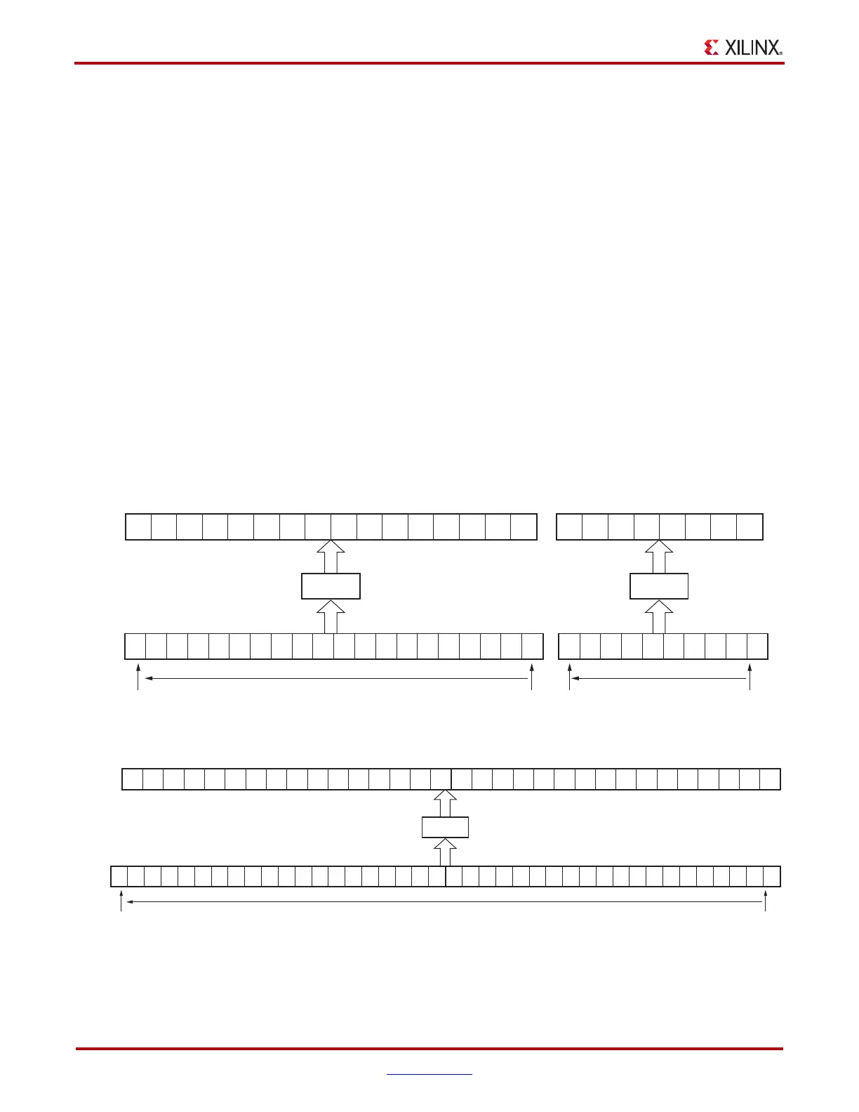
8B/10B Decoder Bit and Byte Order
8B/10B requires bit a0 to be received first, but the GTX transceiver always receives the
right-most bit first. Consequently, the 8B/10B decoder is designed to automatically reverse
the bit order of received data before decoding it. Similarly, because the GTX transceiver
receives the right-most bit first, when a 2-byte interface is used, the first byte received (byte
0) is presented on RXDATA[7:0], and the second byte is presented on RXDATA[15:8].
When a 4-byte interface is used, the first received byte is presented on RXDATA[23:16], and
the fourth byte is presented on RXDATA[31:24]. Figure 4-29 shows how the decoder maps
10-bit data to 8-bit values.
X-Ref Target - Figure 4-29
Figure 4-29: RX Interface with 8B/10B Decoding
15 14 13 1211109876543 210
H
1
G
1
F
1
E
1
D
1
C
1
B
1
A
1
H
0
G
0
F
0
E
0
D
0
C
0
B
0
A
0
H
0
G
0
F
0
E
0
D
0
C
0
B
0
A
0
76543 210
RX_DATA_WIDTH = 20
RXDATA
RX_DATA_WIDTH = 10
UG366_c4_26_051509
Received
Last
Received
Last
Received
First
Received
First
8B/10B
g
0
h
0
j
0
f
0
i
0
e
0
d
0
c
0
b
0
a
0
g
0
h
0
j
0
f
0
i
0
e
0
d
0
c
0
b
0
a
0
g
1
h
1
j
1
f
1
i
1
e
1
d
1
c
1
b
1
a
1
15 14 13 1211109876543 210
H
1
G
1
F
1
E
1
D
1
C
1
B
1
A
1
H
0
G
0
F
0
E
0
D
0
C
0
B
0
A
0
RX_DATA_WIDTH = 40
Received
Last
Received
First
8B/10B
g
0
h
0
j
0
f
0
i
0
e
0
d
0
c
0
b
0
a
0
g
1
h
1
j
1
f
1
i
1
e
1
d
1
c
1
b
1
a
1
31 3029282726252423 22 21 20 19 18 17 16
H
3
G
3
F
3
E
3
D
3
C
3
B
3
A
3
H
2
G
2
F
2
E
2
D
2
C
2
B
2
A
2
RXDATA
g
2
h
2
j
2
f
2
i
2
e
2
d
2
c
2
b
2
a
2
g
3
h
3
j
3
f
3
i
3
e
3
d
3
c
3
b
3
a
3
8B/10B

 Loading...

