108 www.xilinx.com Virtex-6 FPGA GTX Transceivers User Guide
UG366 (v2.5) January 17, 2011
Chapter 2: Shared Transceiver Features
Single External Reference Clock Use Model
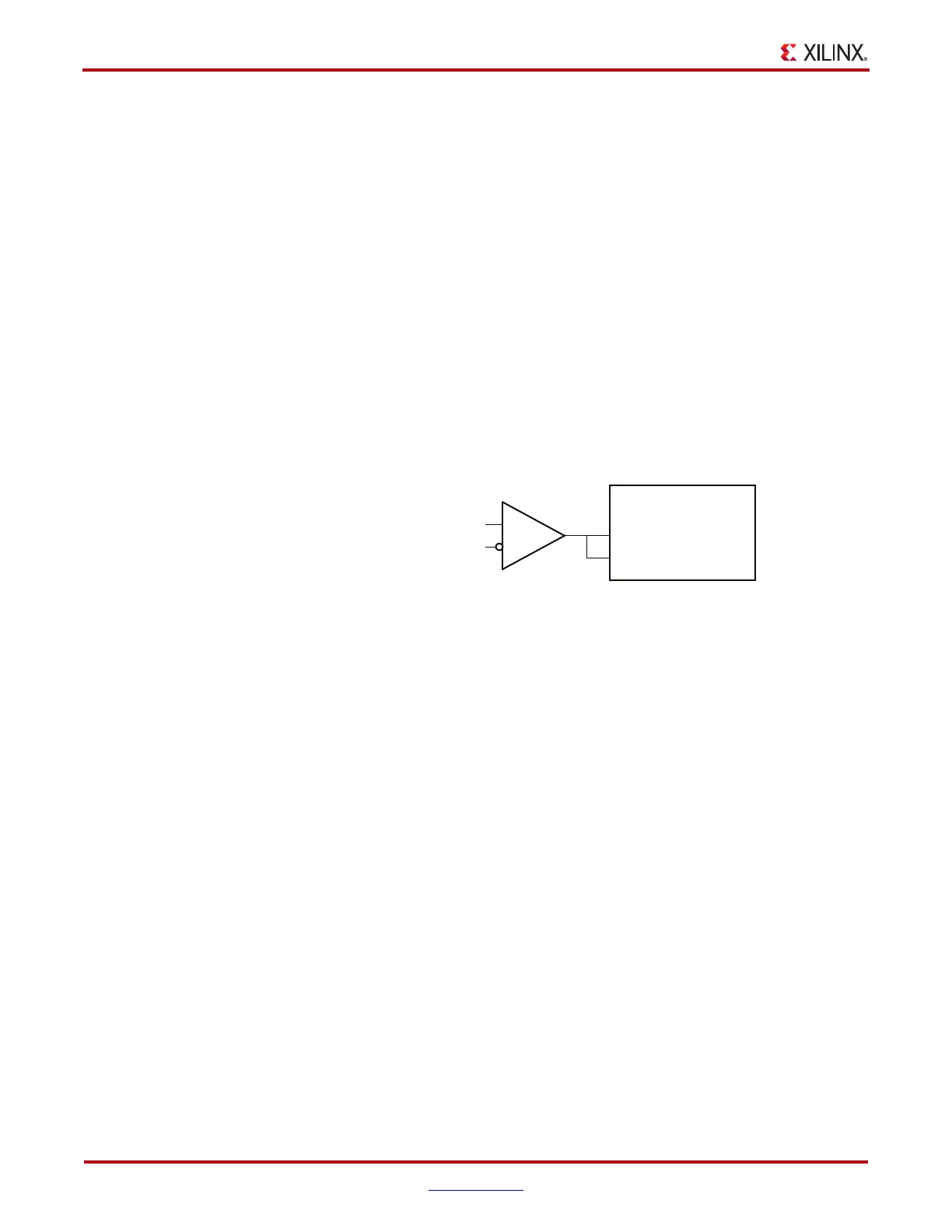
Each Quad has two dedicated differential reference clock inputs (MGTREFCLK0[P/N] or
MGTREFCLK1[P/N]) that can be connected to external clock sources. An IBUFDS_GTXE1
primitive must be instantiated to use these dedicated reference clock pin pairs. The user
design connects the IBUFDS_GTXE1 output (O) to the MGTREFCLKRX[0] and
MGTREFCLKTX[0] ports of the GTXE1 primitive. MGTREFCLKTX[0] must be connected
even if the TX PLL is not used in the design. The IBUFDS_GTXE1 input pins are
constrained in the User Constraints File (UCF). For details about placement constraints
and restrictions on clocking resources (MMCM, BUFGCTRL, IBUFDS_GTXE1, BUFG, etc.),
refer to the Virtex-6 FPGA Clocking Resources User Guide.
The simulation-only attributes must be set on the GTXE1 primitive to match the clock input
used. For the single external reference clock use model, the following settings must be
applied (these are the default settings):
•SIM_RXREFCLK_SOURCE = 000
• SIM_TXREFCLK_SOURCE = 000
Figure 2-4 shows a single reference clock connected to a single GTX transceiver.
Note:
The IBUFDS_GTXE1 diagram in Figure 2-4 is a simplification. The output port ODIV2 is left
floating, and the input port CEB is set to logic 0.
Figure 2-5 shows a single reference clock connected to multiple GTX transceivers.
X-Ref Target - Figure 2-4
Figure 2-4: Single External Reference Clock
MGTREFCLKTX[0]
IBUFDS_GTXE1
I
IB
GTX Transceiver
UG366_c2_03_051509
MGTREFCLKRX[0]
O
MGTREFCLKP
MGTREFCLKN

 Loading...

