Virtex-6 FPGA GTX Transceivers User Guide www.xilinx.com 109
UG366 (v2.5) January 17, 2011
Reference Clock Selection
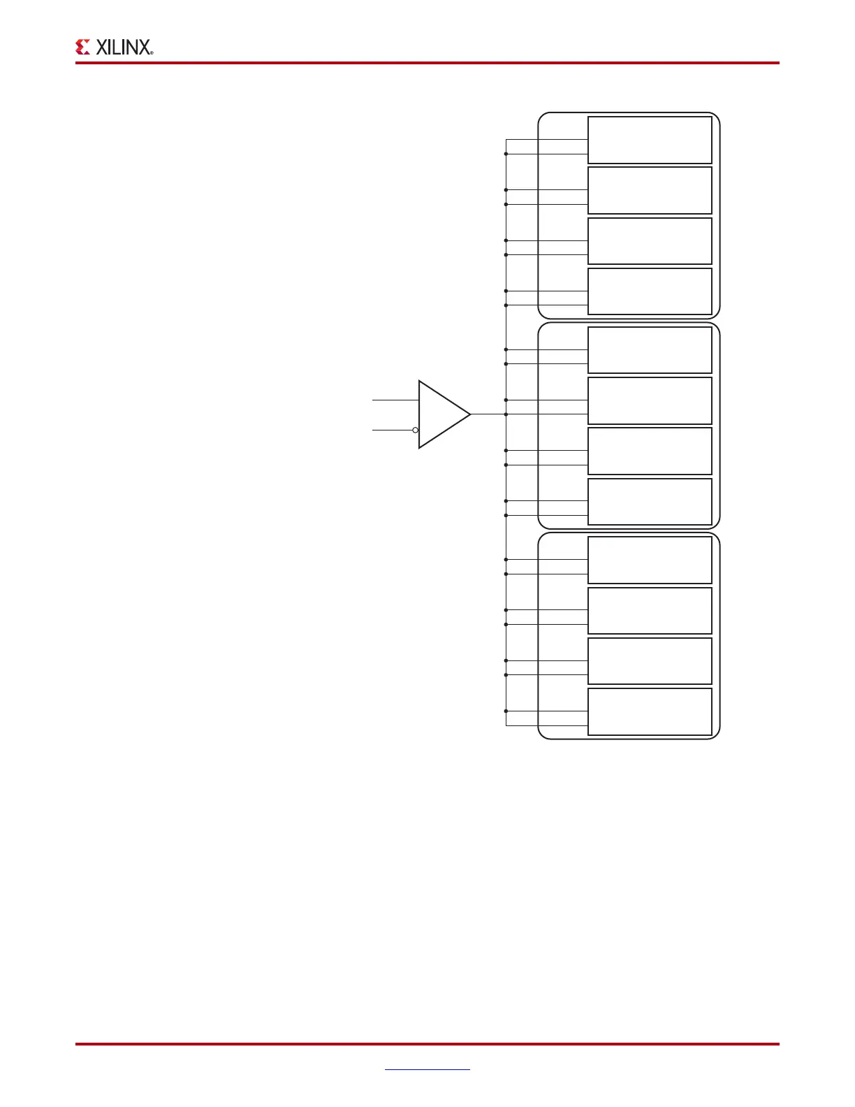
Note: The IBUFDS_GTXE1 diagram in Figure 2-5 is a simplification. The output port ODIV2 is left
floating, and the input port CEB is set to logic 0.
The Xilinx implementation tools make the necessary adjustments to the north/south
routing shown in Figure 2-2 as well as pin swapping necessary to the GTX clock inputs to
route clocks from one Quad to another when required.
The following rules must be observed when sharing a reference clock to ensure that jitter
margins for high-speed designs are met:
1. The number of Quads above the sourcing Quad must not exceed one.
2. The number of Quads below the sourcing Quad must not exceed one.
X-Ref Target - Figure 2-5
Figure 2-5: Multiple GTX Transceivers with Shared Reference Clock
GTXE1
MGTREFCLKTX[0]
MGTREFCLKRX[0]
Q
(n+1)
GTXE1
MGTREFCLKTX[0]
MGTREFCLKRX[0]
GTXE1
MGTREFCLKTX[0]
MGTREFCLKRX[0]
GTXE1
MGTREFCLKTX[0]
MGTREFCLKRX[0]
GTXE1
MGTREFCLKTX[0]
MGTREFCLKRX[0]
O
I
IB
Q
(n)
GTXE1
MGTREFCLKTX[0]
MGTREFCLKRX[0]
MGTREFCLKP
MGTREFCLKN
IBUFDS_GTXE1
UG366_c2_04_071009
GTXE1
MGTREFCLKTX[0]
MGTREFCLKRX[0]
GTXE1
MGTREFCLKTX[0]
MGTREFCLKRX[0]
GTXE1
MGTREFCLKTX[0]
MGTREFCLKRX[0]
Q
(n–1)
GTXE1
MGTREFCLKTX[0]
MGTREFCLKRX[0]
GTXE1
MGTREFCLKTX[0]
MGTREFCLKRX[0]
GTXE1
MGTREFCLKTX[0]
MGTREFCLKRX[0]

 Loading...

