Virtex-6 FPGA GTX Transceivers User Guide www.xilinx.com 153
UG366 (v2.5) January 17, 2011
TX Buffer
TX Buffer
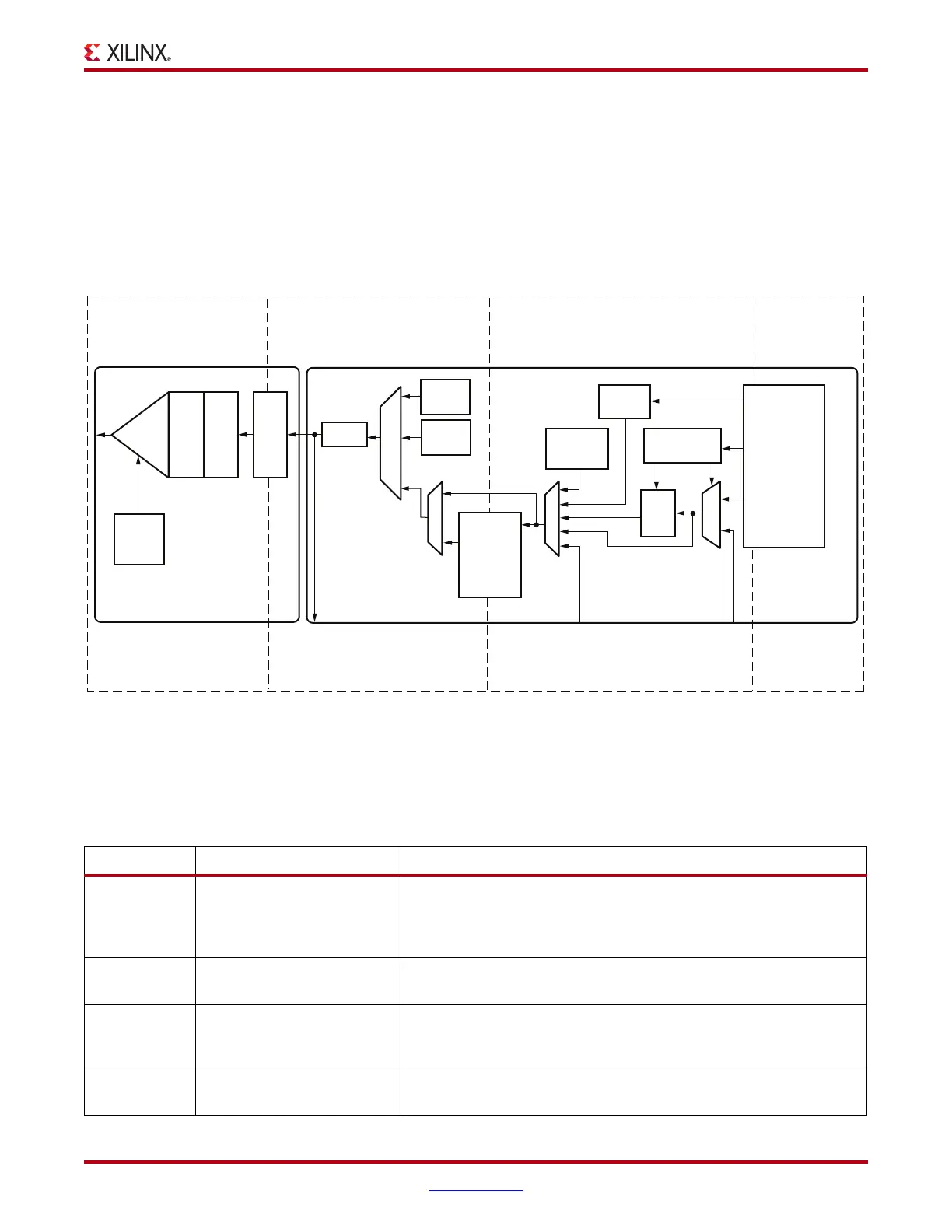
Functional Description
The GTX TX datapath has two internal parallel clock domains used in the PCS: the PMA
parallel clock domain (XCLK) and the TXUSRCLK domain. To transmit data, the XCLK
rate must match the TXUSRCLK rate, and all phase differences between the two domains
must be resolved. Figure 3-20 shows the XCLK and TXUSRCLK domains.
The GTX transmitter includes a TX buffer and a TX phase-alignment circuit to resolve
phase differences between the PMACLK and TXUSRCLK domains. All TX datapaths must
use these circuits. Table 3-15 shows trade-offs between buffering and phase alignment.
X-Ref Target - Figure 3-20
Figure 3-20: TX Clock Domains
TX Serial Clock
TX-PMA
TX-PCS
TX
Driver
PMA
PLL
Divider
TX
OOB
and
PCIe
PISO
Polarity
Phase
Adjust
FIFO &
Over-
sampling
Pattern
Generator
8B
/
10B
TX PIPE
CONTROL
FPGA
TX
Interface
PMA Parallel Clock
(XCLK)
PCS Parallel Clock
(TXUSRCLK)
FPGA
Parallel Clock
(TXUSRCLK2)
UG366_c3_10_051509
TX
Gearbox
SATA
OOB
TX
Pre/
Post
Emp
PCIe
Beacon
From RX
Parallel Data
(Far-End PCS
Loopback)
From RX
Parallel Data
(Far-End PMA
Loopback)
To RX Parallel
Data (Near-End
PCS Loopback)
Table 3-15: Buffering vs. Phase Alignment
TX Buffer TX Phase Alignment
Ease of Use The TX buffer is used when
possible. It is robust and easy
to operate.
Phase alignment requires extra logic and additional constraints on
clock sources. TXOUTCLK cannot be used unless the
TXOUTCLK_CTRL attribute is set to “TXPLLREFCLK_DIV1” or
“TXPLLREFCLK_DIV2”.
Latency If low latency is critical, the
TX buffer must be bypassed.
Phase alignment uses fewer registers in the datapath.
TX Lane-to-
Lane Deskew
The phase-alignment circuit can be used to reduce the skew between
separate GTX transceivers. All GTX transceivers involved must use
the same line rate.
Oversampling The TX buffer is required for
oversampling.

 Loading...

