Virtex-6 FPGA GTX Transceivers User Guide www.xilinx.com 169
UG366 (v2.5) January 17, 2011
TX Fabric Clock Output Control
• TXOUTCLKPMA_DIV1/DIV2: This is the divided down PLL clock after the TX phase
interpolator and is used by the TX PCS block. The TX phase interpolator is used to
match the phase of the internal clock to the FPGA logic clock in TX buffer bypass
mode.
• TXPLLREFCLK_DIV1/DIV2: This is the input reference clock to the TX PLL.
TXPLLREFCLK is the recommended clock for general usage and is required for the
TX buffer bypass mode.
The TXOUTCLKPMA_DIV2 output is the 2-byte datapath frequency and is used when
TXDATA is 2 bytes. The TXOUTCLKPMA_DIV1 output is the 1-byte datapath frequency
and is used when TXDATA is 1 byte.
Ports and Attributes
Table 3-29 defines the TX Fabric Clock Output Control block ports.
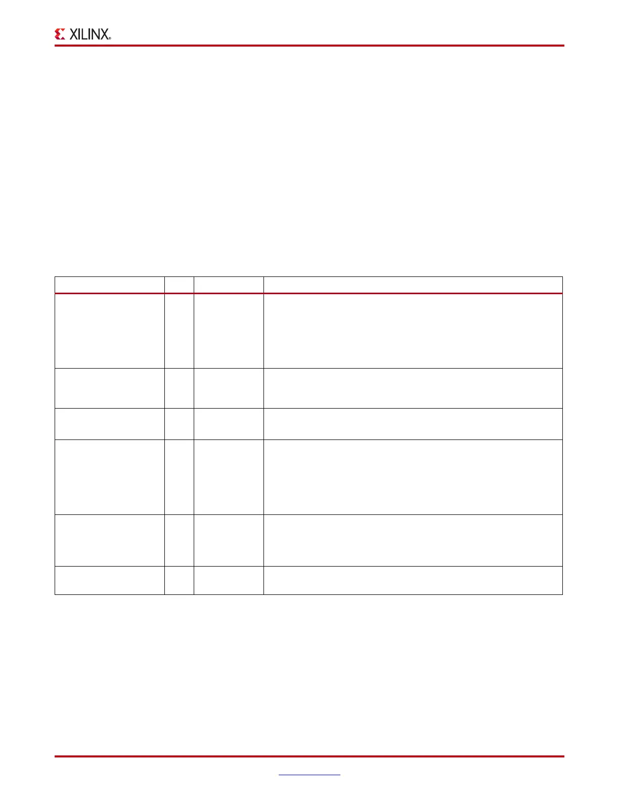
Table 3-29: TX Fabric Clock Output Control Ports
Port Dir Clock Domain Description
GTXTEST[1] In Async This port resets the TX PLL output divider (controlled via the
TXPLL_DIVSEL_OUT attribute or the TXRATE port). The TX PLL
output clock divider must be reset whenever the line rate is changed
by modifying the output dividers at run time. To perform this reset,
GTXTEST[1] is asserted for 16 TXUSRCLK2 cycles after the line rate
change is completed.
MGTREFCLKFAB[0] Out Async MGTREFCLKFAB[0] is a redundant output. TXOUTCLK with
TXOUTCLK_CTRL = “TXPLLREFCLK_DIV1” should be used
instead.
O
ODIV2
Out Async The IBUFDS_GTXE1 primitive allows MGTREFCLK to be output to
the FPGA logic directly.
PHYSTATUS Out RXUSRCLK2
/Async
After TXRATE is changed to initiate a rate change, PHYSTATUS is
output Low and toggles for one TXUSRCLK2 cycle at the conclusion
of the rate change as defined by TRANS_TIME_RATE. PHYSTATUS
is intended for PCI Express protocol operation. Non PCI Express
protocol operation should monitor TXRATEDONE. Refer to
Table 3-33, page 179 for more information on PHYSTATUS.
TXOUTCLK Out Async TXOUTCLK is the recommended clock output to the FPGA logic. The
TXOUTCLK_CTRL attribute is the input selector for TXOUTCLK
and allows the TX PLL input reference clock or other internal clocks
to be output to the FPGA logic.
TXOUTCLKPCS Out Async TXOUTCLKPCS is a redundant output. TXOUTCLK with
TXOUTCLK_CTRL = “TXOUTCLKPCS” should be used instead.

 Loading...

