Virtex-6 FPGA GTX Transceivers User Guide www.xilinx.com 131
UG366 (v2.5) January 17, 2011
FPGA TX Interface
Table 3-6 defines the FPGA TX Interface attributes.
Using TXOUTCLK to Drive the GTX TX
Figure 3-2 through Figure 3-7 show different ways that FPGA clock resources can be used
to drive the parallel clocks for the TX interface. In these examples, the TXOUTCLK port is
derived from MGTREFCLK0[P/N] or MGTREFCLK1[P/N], and the TXOUTCLK_CTRL
attribute is set to “TXPLLREFCLK_DIV1”.
• Depending on the input reference clock frequency and the required line rate, an
MMCM and the appropriate TXOUTCLK_CTRL attribute setting is required. The
CORE Generator™ tool creates a sample design based on different design
requirements for most cases.
• When the TXOUTCLK_CTRL attribute is set to “TXOUTCLKPMA_DIV1”, the
MMCM is required.
• In use models where the TX buffer is bypassed, there are additional restrictions on the
clocking resources. Refer to TX Buffer Bypass, page 155 for more information.
TXOUTCLK Driving a GTX TX in 2-Byte Mode (Single Lane)
In Figure 3-2, TXOUTCLK is used to drive TXUSRCLK2 for 2-byte mode
(TX_DATA_WIDTH = 16 or 20). The GEN_TXUSRCLK attribute is set to “TRUE”, and the
TXUSRCLK input port is tied to ground. TXUSRCLK is internally generated for the
internal TX PCS datapath.
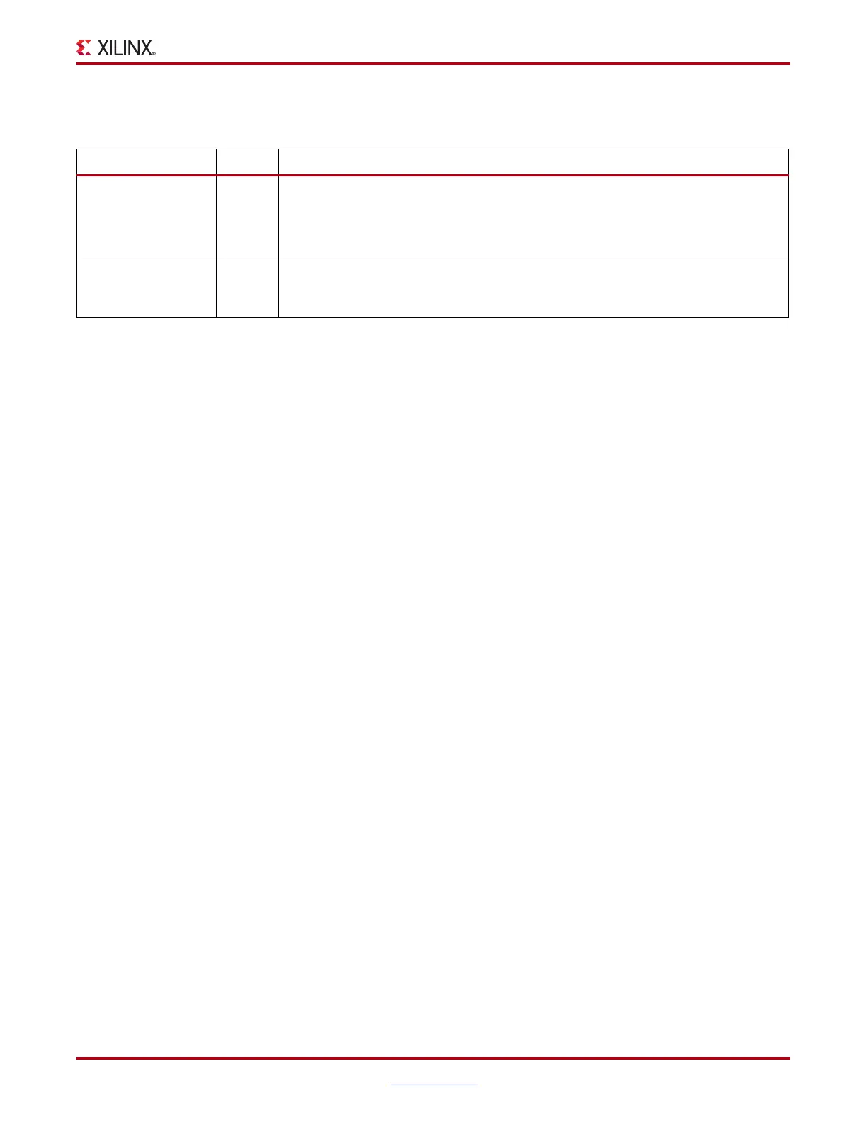
Table 3-6: FPGA TX Interface Attributes
Attribute Type Description
GEN_TXUSRCLK Boolean Controls internal generation of TXUSRCLK available in certain modes of operation.
See TXUSRCLK and TXUSRCLK2 Generation, page 129 for more details.
TRUE: TXUSRCLK internally generated. TXUSRCLK must be tied Low.
FALSE: TXUSRCLK must be provided by user.
TX_DATA_WIDTH Integer Sets the bit width of the TXDATA port. When 8B/10B encoding is enabled,
TX_DATA_WIDTH must be set to 10, 20, or 40. Valid settings are 8, 10, 16, 20, 32, and
40. See Interface Width Configuration, page 128 for more details.

 Loading...

