Virtex-6 FPGA GTX Transceivers User Guide www.xilinx.com 115
UG366 (v2.5) January 17, 2011
PLL
The Virtex-6 FPGA GTX transceiver allows the N1 divider to be set independently from
the PCS internal datapath width. This allows additional flexibility in reference clock
selection.
Ports and Attributes
Table 2-8 defines the PLL ports.
Table 2-9 defines the PLL attributes.
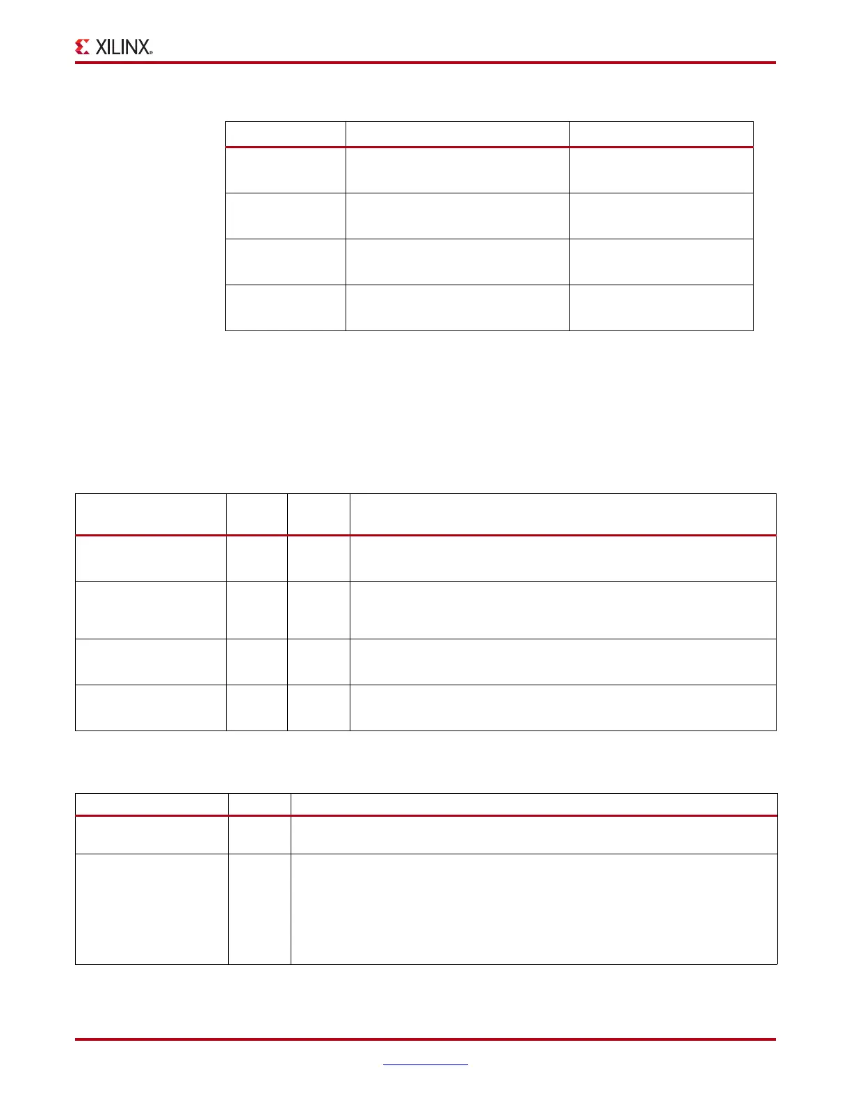
Table 2-7: PLL Divider Attribute and Common Values
Factor Attribute Name Valid Settings
M TXPLL_DIVSEL_REF
RXPLL_DIVSEL_REF
1, 2
N1 TXPLL_DIVSEL45_FB
RXPLL_DIVSEL45_FB
4, 5
N2 TXPLL_DIVSEL_FB
RXPLL_DIVSEL_FB
2, 4, 5
D TXPLL_DIVSEL_OUT
RXPLL_DIVSEL_OUT
1, 2, 4
Table 2-8: PLL Ports
Port Dir
Clock
Domain
Description
PLLTXRESET
PLLRXRESET
In Async These active-High PLL ports reset the dividers inside the PLL as well as
the PLL lock indicator block.
TXPLLLKDET
RXPLLLKDET
Out Async This active-High PLL frequency lock signal indicates that the PLL
frequency is within predetermined tolerance. The GTX transceiver and
its clock outputs are not reliable until this condition is met.
TXPLLLKDETEN
RXPLLLKDETEN
In Async This port enables the PLL lock detector and must always be tied High.
TXPLLPOWERDOWN
RXPLLPOWERDOWN
In Async These active-High PLL signals provide power down.
Table 2-9: PLL Attributes
Attribute Type Description
PMA_CFG 76-bit
Binary
Reserved. Use only recommended values from the Virtex-6 FPGA GTX
Transceiver Wizard.
TX_CLK_SOURCE String This attribute is the multiplexer select signal in Figure 2-8, which determines
whether the TX PLL or the RX PLL supplies the clock for the TX datapath.
For applications where TX and RX have the same line rate with a small frequency
offset, using the RX PLL to supply both the TX and RX datapaths allows some
power savings.
Valid values are “TXPLL” and “RXPLL”.

 Loading...

