114 www.xilinx.com Virtex-6 FPGA GTX Transceivers User Guide
UG366 (v2.5) January 17, 2011
Chapter 2: Shared Transceiver Features
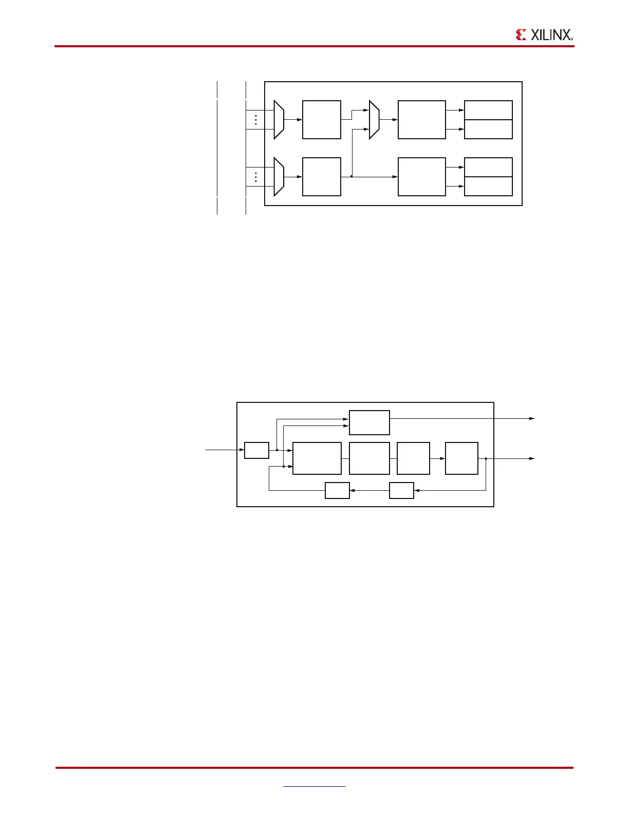
The PLL input clock selection is described in Reference Clock Selection, page 102. The PLL
outputs feed the TX and RX clock divider blocks, which control the generation of serial and
parallel clocks used by the PMA and PCS blocks. These blocks are described in TX Fabric
Clock Output Control, page 167 and RX Fabric Clock Output Control, page 207.
Figure 2-9 illustrates a conceptual view of the PLL architecture. A low phase noise PLL
input clock is recommended for the best jitter performance. The input clock can be divided
by a factor of M before feeding into the phase frequency detector. The feedback dividers,
N1 and N2, determine the VCO multiplication ratio and the PLL output frequency. A lock
indicator block compares the frequencies of the reference clock and the VCO feedback
clock to determine if a frequency lock has been achieved.
Note:
In Figure 2-9, a value of 4 or 5 for the feedback divider (N1*N2) of the PLL is not supported.
Equation 2-1 shows how to determine the PLL output frequency (GHz).
Equation 2-1
Equation 2-2 shows how to determine the line rate (Gb/s). D is the PLL output divider that
resides in the clock divider block.
Equation 2-2
Table 2-7 lists the actual attribute and commonly used divider values.
X-Ref Target - Figure 2-8
Figure 2-8: Top-Level PLL Architecture
X-Ref Target - Figure 2-9
Figure 2-9: PLL Detail
REFCLK Distribution
TX
PLL
RX
PLL
TX
Clock
Dividers
RX
Clock
Dividers
TX PMA
TX PCS
RX PMA
RX PCS
UG366_c2_05_051509
PLL
CLKIN
/ M
Lock
Indicator
Phase
Frequency
Detector
Charge
Pump
Loop
Filter
VCO
PLL
LOCKED
PLL
CLKOUT
/ N1/ N2
UG366_c2_06_051509
f
PLLClkout
f
PLLClkin
N1 N2
M
----------------------
=
f
LineRate
f
PLLClkout
2
D
-----------------------------------=

 Loading...

