270 www.xilinx.com Virtex-6 FPGA GTX Transceivers User Guide
UG366 (v2.5) January 17, 2011
Chapter 4: Receiver
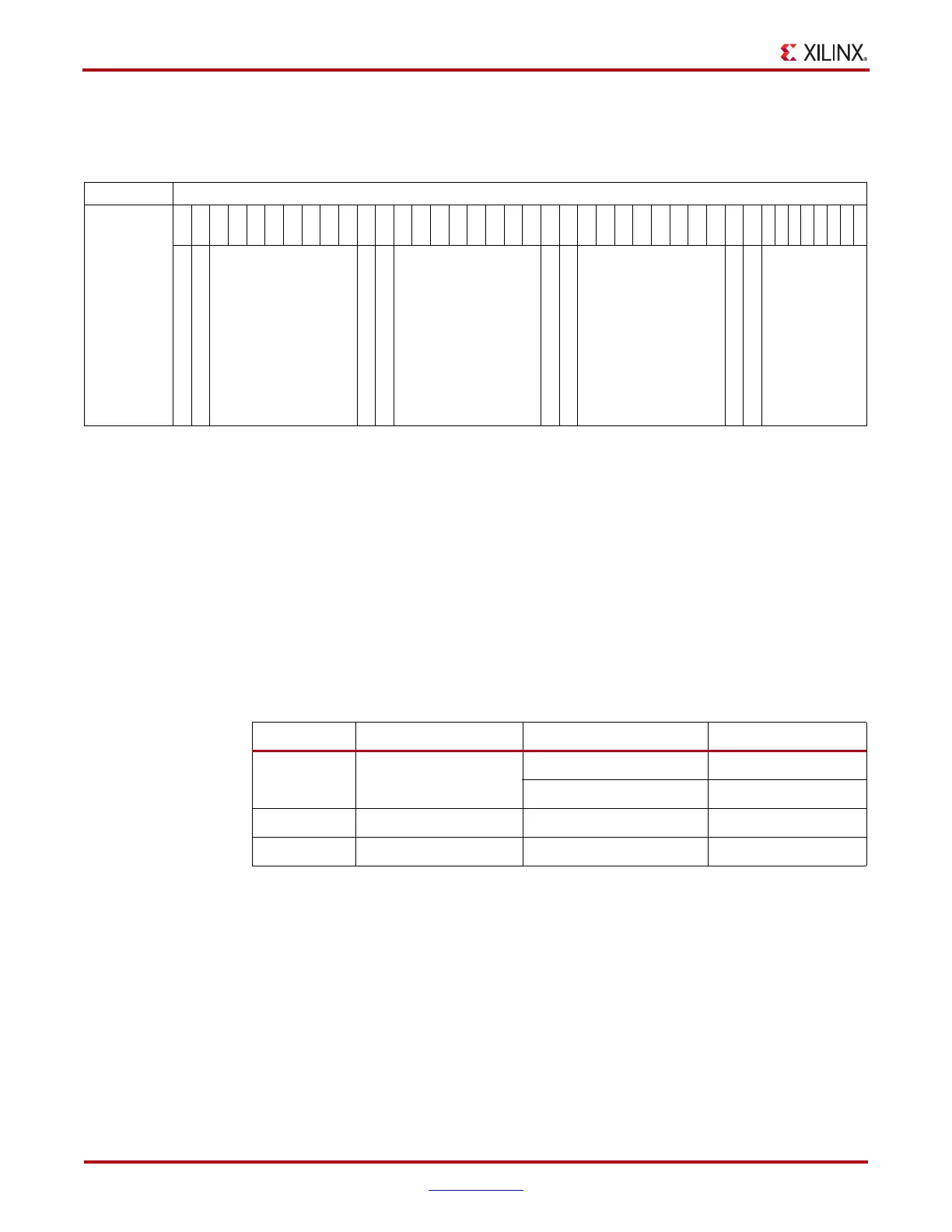
16 to 20 bits, or 32 to 40 bits. Table 4-57 shows the data received when the 8B/10B decoder
is disabled.
RXUSRCLK and RXUSRCLK2 Generation
The FPGA RX interface includes two parallel clocks: RXUSRCLK and RXUSRCLK2.
RXUSRCLK is the internal clock for the PCS logic in the GTX receiver. The required rate for
RXUSRCLK depends on the internal datapath width of the GTXE1 primitive and the RX
line rate of the GTX receiver. Equation 4-1 shows how to calculate the required rate for
RXUSRCLK.
Equation 4-1
RXUSRCLK can be generated internally to the GTX transceiver. This functionality is
controlled by the GEN_RXUSRCLK attribute. Table 4-58 describes the situations in which
RXUSRCLK can be generated internally by the GTX transceiver. In these cases, the
RXUSRCLK port must be tied Low.
RXUSRCLK2 is the main synchronization clock for all signals into the RX side of the GTX
transceiver. Most signals into the RX side of the GTX transceiver are sampled on the
positive edge of RXUSRCLK2. RXUSRCLK2 and RXUSRCLK have a fixed-rate
relationship based on the RX_DATA_WIDTH setting. Table 4-59 shows the relationship
between RXUSRCLK2 and RXUSRCLK per RX_DATA_WIDTH values.
Table 4-57: RX Data Received with 8B/10B Decoder Bypassed
< < Data reception order is right to left < <
Data
Received
3
9
3
8
3
7
3
6
3
5
3
4
3
3
3
2
3
1
3
0
2
9
2
8
2
7
2
6
2
5
2
4
2
3
2
2
2
1
2
0
1
9
1
8
1
7
1
6
1
5
1
4
1
3
1
2
1
1
1
0
9 8 76543210
RXDISPERR[3]
RXCHARISK[3]
RXDATA[31:24]
RXDISPERR[2]
RXCHARISK[2]
RXDATA[23:16]
RXDISPERR[1]
RXCHARISK[1]
RXDATA[15:8]
RXDISPERR[0]
RXCHARISK[0]
RXDATA[7:0]
Table 4-58: RXUSRCLK Internal Generation Configurations
RX_DATA_WIDTH GTX Lanes in Channel
(1)
GEN_RXUSRCLK
1-Byte 8, 10
1TRUE
2 or more FALSE
2-Byte 16, 20 1 or more TRUE
4-Byte 32, 40 1 or more FALSE
Notes:
1. For single lane protocols such as 1 Gb/s Ethernet, “GTX Lanes in Channel” is 1. For multiple lane
protocols like XAUI, “GTX Lanes in Channel” is 2 or more.
RXUSRCLK Rate
Line Rate
Internal Datapath Width
--------------------------------------------------------------------=

 Loading...

