238 www.xilinx.com Virtex-6 FPGA GTX Transceivers User Guide
UG366 (v2.5) January 17, 2011
Chapter 4: Receiver
RX Elastic Buffer
Functional Description
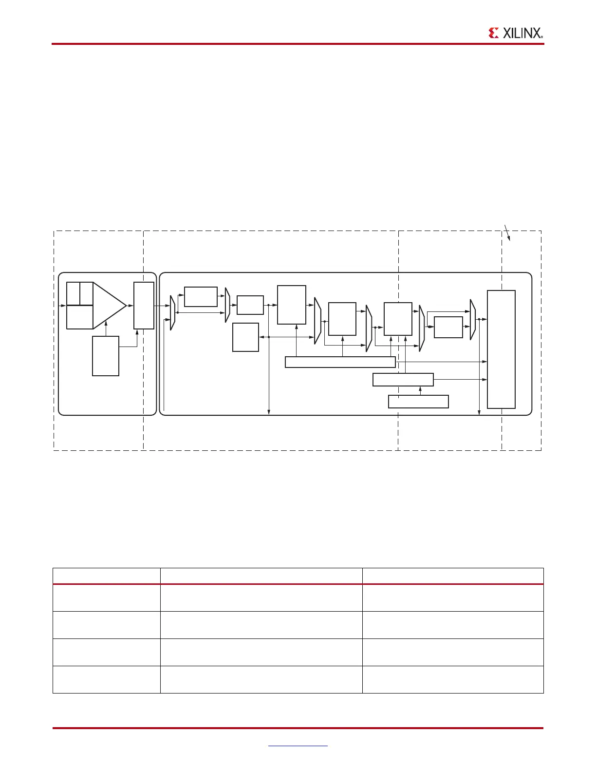
The GTX RX datapath has two internal parallel clock domains used in the PCS: the PMA
parallel clock domain (XCLK) and the RXUSRCLK domain. To receive data, the PMA
parallel rate must be sufficiently close to the RXUSRCLK rate, and all phase differences
between the two domains must be resolved. Figure 4-34 shows the two parallel clock
domains, XCLK and RXUSRCLK.
The GTX transceiver includes an RX elastic buffer to resolve differences between the
PMACLK and RXUSRCLK domains. The phase of the two domains can also be matched
by using the recovered clock from the transceiver to drive RXUSRCLK and adjusting its
phase to match XCLK (see RX Buffer Bypass, page 231). All RX datapaths must use one of
these approaches. The costs and benefits of each approach are shown in Table 4-42.
X-Ref Target - Figure 4-34
Figure 4-34: RX Clock Domain
UG366_c4_31_011111
PMA Parallel Clock
(XCLK)
RX Serial Clock
PCS Parallel
Clock
(RXUSRCLK)
FPGA
Parallel Clock
(RXUSRCLK2)
RX-PMA
RX-PCS
RX
EQ
RX
OOB
SIPO
10B/8B
Decoder
FPGA
RX
Interface
Polarity
Over-
sampling
Loss of Sync
RX Status Control
PRBS
Checker
RX
CDR
Shared
PMA
PLL
Divider
Comma
Detect
and
Align
RX
Elastic
Buffer
D
F
E
RX
Gearbox
From TX Parallel
Data (Near-End
PCS Loopback)
To TX Parallel
Data (Far-End
PMA Loopback)
RX PIPE Control
To TX Parallel
Data (Far-End)
PCS Loopback)
Table 4-42: Buffering vs. Phase Alignment
RX Elastic Buffer RX Phase Alignment
Clocking Options Can use recovered clock or local clock (with
clock correction)
Must use recovered clock
Initialization Works immediately Must wait for all clocks to stabilize then
perform alignment procedure
Latency Buffer latency depends on features used (clock
correction and channel bonding)
Lower deterministic latency than using the
RX elastic buffer
Clock Correction /
Channel Bonding
Required for clock correction / channel
bonding

 Loading...

