194 www.xilinx.com Virtex-6 FPGA GTX Transceivers User Guide
UG366 (v2.5) January 17, 2011
Chapter 4: Receiver
RX Equalizer
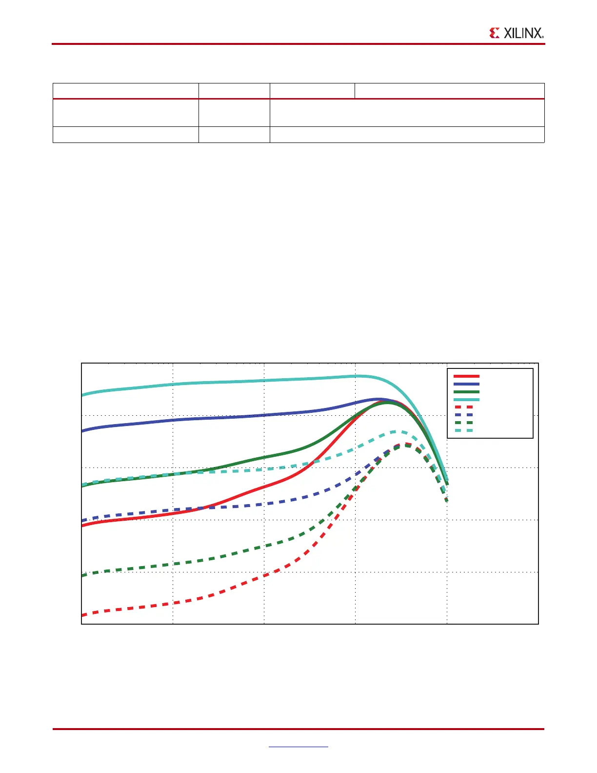
Functional Description
The RX has a continuous time RX equalization circuit and a decision feedback equalization
circuit to compensate for high-frequency losses in the channel.
This continuous time RX equalization circuit can be tuned to meet the specific
requirements of the physical channel used in the design by compensating for signal
distortion due to high-frequency attenuation.
It is a 3-stage amplifier with the ability to boost the input signal at low, intermediate, and
high frequencies. There are eight different frequency responses to accommodate several
channels.
SATA_MIN_INIT 6-bit Hex Lower bound on idle count during COMINIT/COMRESET for
SAS/SATA
SATA_MIN_WAKE 6-bit Hex Lower bound on idle count during COMWAKE for SAS/SATA
Notes:
1. These are OOB nominal values. Consult the Virtex-6 FPGA Data Sheet for OOB specifications.
Table 4-10: RX OOB Attributes (Cont’d)
Attribute Type Description
X-Ref Target - Figure 4-9
Figure 4-9: Absolute Gain (Voltage Transfer Function)
Frequency (Hz)
10
6
10
7
10
8
10
9
10
10
10
11
UG366_c4_08_051509
Gain (dB)
10
5
0
-5
-10
-15
RXEQMIX = 000
RXEQMIX = 001
RXEQMIX = 010
RXEQMIX = 011
RXEQMIX = 100
RXEQMIX = 110
RXEQMIX = 111
RXEQMIX = 101

 Loading...

