Virtex-6 FPGA GTX Transceivers User Guide www.xilinx.com 315
UG366 (v2.5) January 17, 2011
Appendix C
Low Latency Design
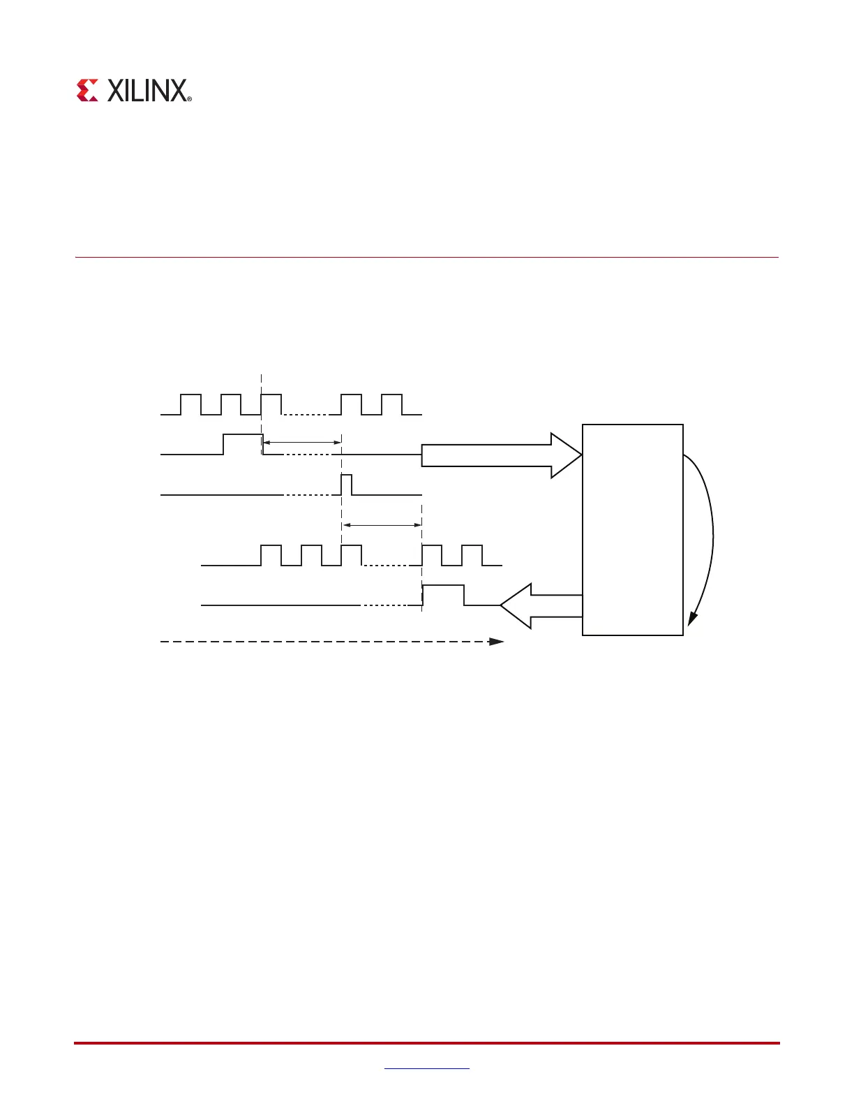
This appendix illustrates the latency of the different functional blocks inside the TX and the
RX sections of the GTX transceiver. Figure C-1 shows a pictorial definition of the TX and
RX latencies.
Each functional block has a latency defined as the time difference between the inputs and
the outputs of the specific block. Some blocks in the GTX transceiver can be bypassed,
reducing the latency of the datapath through the transmitter or the receiver. The latency of
the blocks is deterministic with the exception of the RX elastic buffer and the TX buffer.
Bypassing buffers requires the phase alignment procedure. Refer to TX Buffer Bypass,
page 155 and RX Buffer Bypass, page 231 for more details.
X-Ref Target - Figure C-1
Figure C-1: Latency Definition
UG198_aC_01_102910
TXUSRCLK
GTX
Transceiver
RX Data
Loopback
TX Data
TX FPGA
Data
RXUSRCLK
RX FPGA
Data
Serial
Data
First serial bit
transmitted/received
Latency RX
Time
Latency TX

 Loading...

