Virtex-6 FPGA GTX Transceivers User Guide www.xilinx.com 167
UG366 (v2.5) January 17, 2011
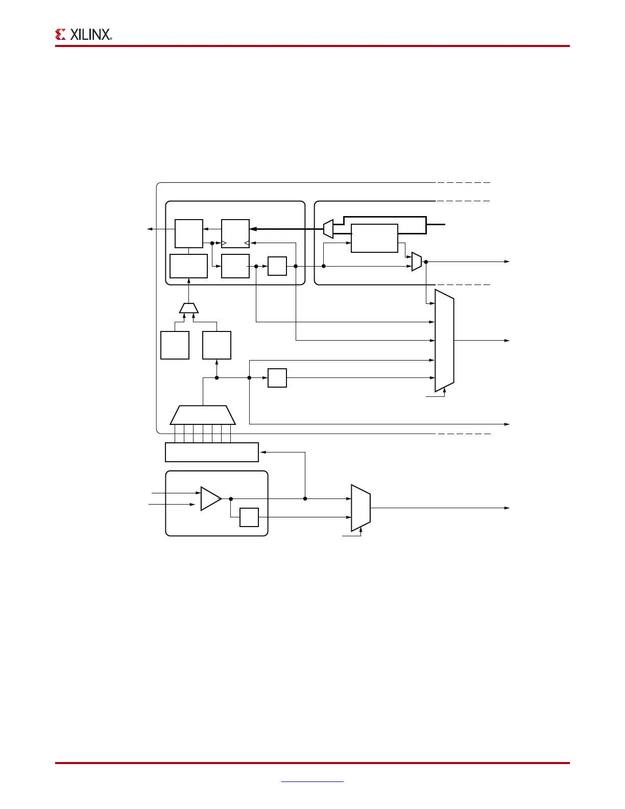
TX Fabric Clock Output Control
TX Fabric Clock Output Control
Functional Description
The TX Fabric Clock Output Control block has two main components: serial clock divider
control and parallel clock divider and selector control. The clock divider and selector
details are illustrated in Figure 3-28.
Notes relevant to Figure 3-28:
1. TXOUTCLKPCS and MGTREFCLKFAB[0] are redundant outputs. Use TXOUTCLK
for new designs.
2. The REFCLK_CTRL option is controlled automatically by software and is not user
selectable. The user can only route one of IBUFDS_GTXE1’s O or ODIV2 outputs to the
fabric.
3. IBUFDS_GTXE1 is a redundant output for additional clocking scheme flexibility.
4. The RX PLL resides in the RX portion of the same GTX transceiver. It can be used in
place of the TX PLL for low-power operation.
X-Ref Target - Figure 3-28
Figure 3-28: TX Serial and Parallel Clock Divider Detail
UG366_c3_18_051809
TX PMA TX PCS
TXOUTCLKPCS
TXOUTCLK
000
001
010
011
100
TXDATA
TXOUTCLKPCS
PISO
REFCLK Distribution
0
1
O
REFCLK Sel
GTXE1 (GTX Transceiver Primitive)
TXP/N
Phase
Interp
TX Over-
sampler
TXDATA From
Upstream
PCS Blocks
/4 or
/5
/D
{1,2,4}
/2
TXOUTCLKPMA_DIV1
TXOUTCLKPMA_DIV2
TXPLLREFCLK_DIV1
TXPLLREFCLK_DIV2
TXOUTCLK_CTRL (Attribute)
TX
PLL
RX
PLL
MGTREFCLKFAB[0]
IBUFDS_GTXE1
Output to Fabric
IBUFDS_GTXE1
MGT
REFCLK
0/1
/2
ODIV2
REFCLK_CTRL
/2
O

 Loading...

