Virtex-6 FPGA GTX Transceivers User Guide www.xilinx.com 209
UG366 (v2.5) January 17, 2011
RX Fabric Clock Output Control
Ports and Attributes
Table 4-24 defines the RX clock divider control block ports.
Table 4-25 defines the RX Clock Divider Control block attributes.
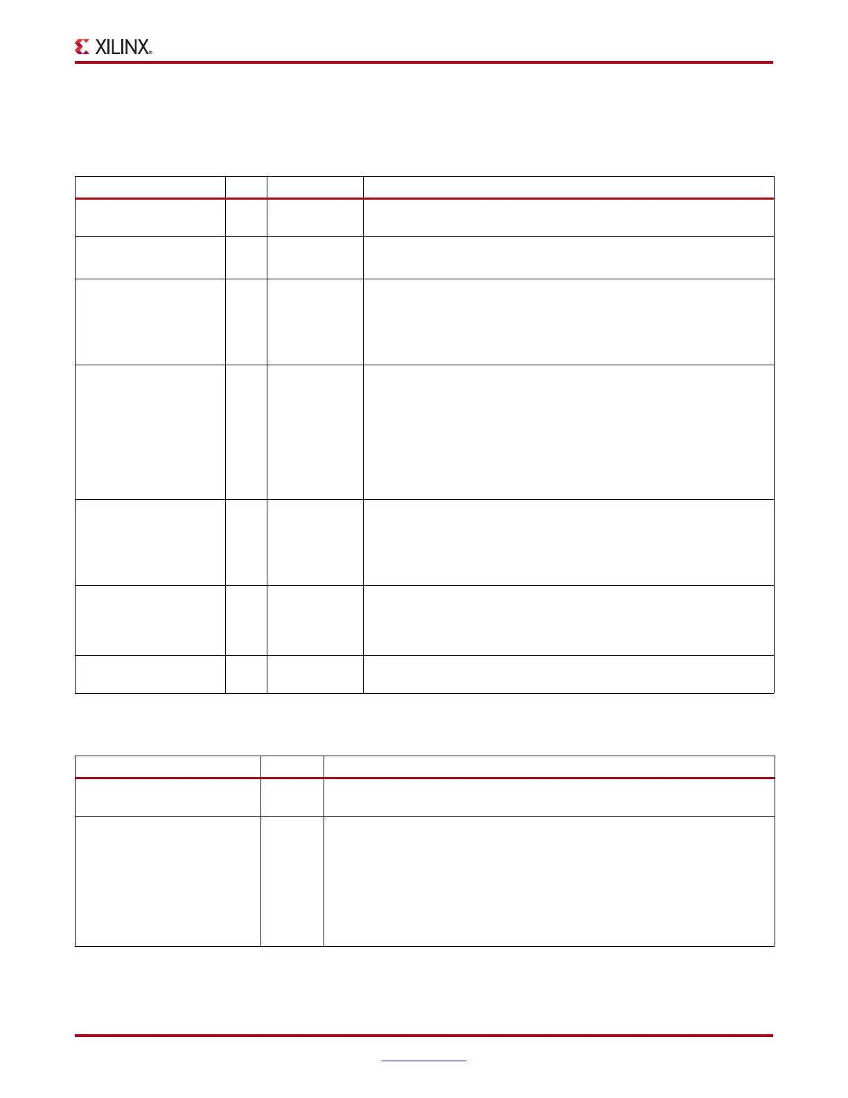
Table 4-24: RX Clock Divider Control Ports
Port Dir Clock Domain Description
MGTREFCLKFAB[1] Out Async This is a redundant output. RXRECCLK with RXRECCLK_CTRL =
“RXPLLREFCLK_DIV1” should be used instead.
O
ODIV2
Out Async The IBUFDS_GTXE1 primitive allows the MGTREFCLK to be output
to the FPGA logic directly.
PHYSTATUS Out RXUSRCLK2 After RXRATE[1:0] is changed to initiate a rate change, PHYSTATUS
goes Low and toggles for one RXUSRCLK2 cycle at the conclusion of
the rate change as defined by TRANS_TIME_RATE. PHYSTATUS is
intended for PCI Express protocol. Non PCI Express protocol should
monitor RXRATEDONE.
RXRATE[1:0] In RXUSRCLK2 Controls the setting for the RX serial clock divider for low line rate
support (see Table 4-23). This input port is used in combination with
the RXPLL_DIVSEL_OUT attribute.
00: Let RXPLL_DIVSEL_OUT determine the D divider value
01: Set the D divider to 4
10: Set the D divider to 2
11: Set the D divider to 1
RXRATEDONE Out RXUSRCLK2 The RXRATEDONE port is asserted High for one RXUSRCLK2 cycle
in response to a change on the RXRATE[1:0] port. The
TRANS_TIME_RATE attribute determines the period of time
between a change on the RXRATE[1:0] port and the assertion of
RXRATEDONE.
RXRECCLK Out Async This is the recommended clock output to the fabric. The attribute
RXRECCLK_CTRL is the input selector for RXRECCLK and allows
the RX PLL input reference clock or the recovered clocks to be output
to fabric.
RXRECCLKPCS Out Async This is a redundant output. RXRECCLK with RXRECCLK_CTRL =
“RXRECCLKPCS” should be used instead.
Table 4-25: RX Clock Divider Control Attributes
Attribute Type Description
RX_EN_RATE_RESET_BUF Boolean When set to TRUE, this attribute enables automatic RX buffer reset during a
rate change event initiated by a change in RXRATE[1:0].
RXPLL_DIVSEL_OUT Integer This controls the setting for the RX serial clock divider for low line rate
support (see Table 4-23). This attribute is only valid when
RXRATE[1:0] = 00. Otherwise the D divider value is controlled by
RXRATE[1:0]. Valid settings are:
1: Set the D divider to 1
2: Set the D divider to 2
4: Set the D divider to 4

 Loading...

