Virtex-6 FPGA GTX Transceivers User Guide www.xilinx.com 283
UG366 (v2.5) January 17, 2011
Power Supply and Filtering
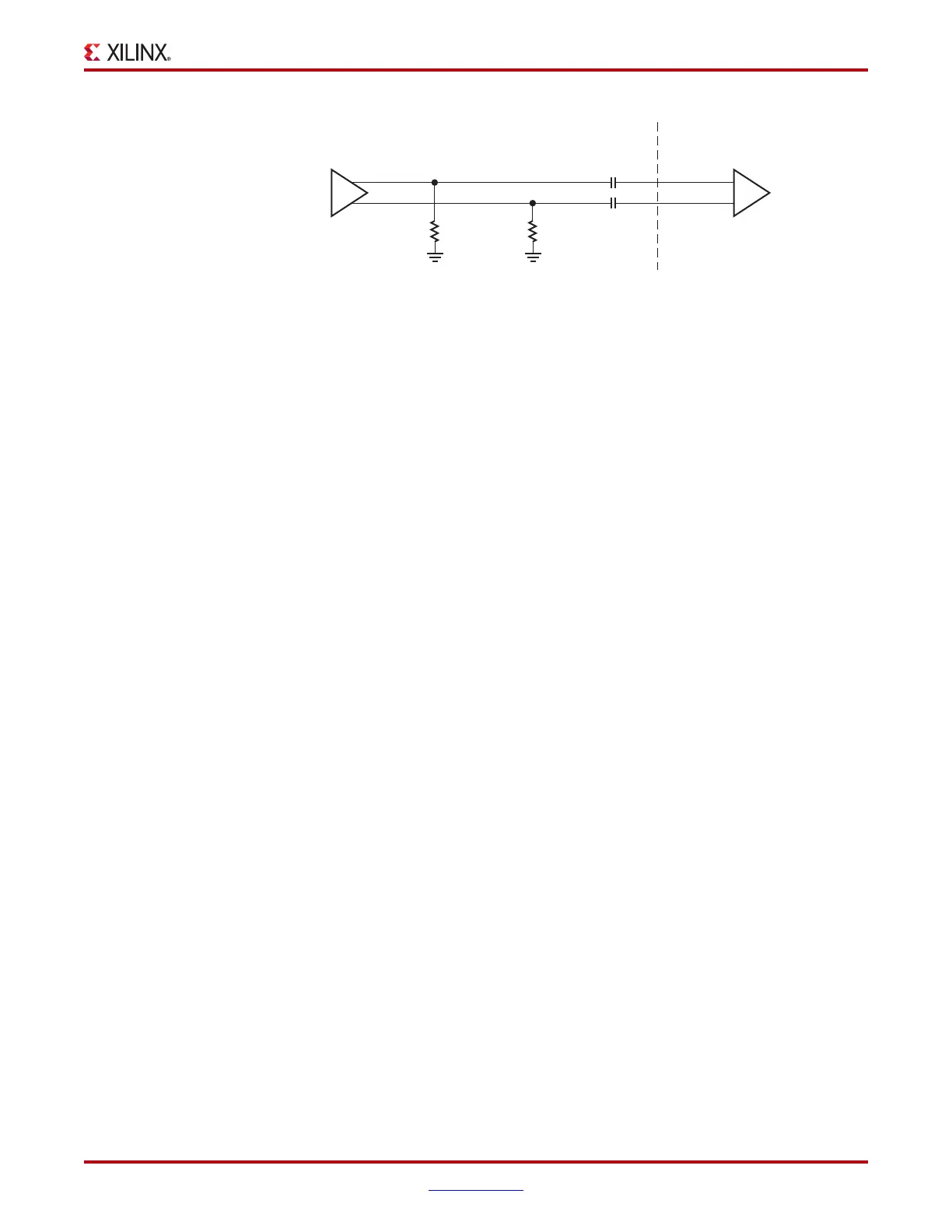
AC Coupled Reference Clock
AC coupling of the oscillator reference clock output to the Quad reference clock inputs
serves multiple purposes:
• DC current is blocked between the oscillator and the Quad dedicated clock input pins
(which reduces the power consumption of both parts as well)
• Common mode voltage independence
• The AC coupling capacitor forms a high-pass filter with the on-chip termination that
attenuates a wander of the reference clock
To minimize noise and power consumption, external AC coupling capacitors between the
sourcing oscillator and the Quad dedicated clock reference clock input pins are required.
Unused Reference Clocks
It is recommended to connect the unused differential input pin clock pair to ground or
leave both MGTREFCLKP and MGTREFCLKN floating.
Reference Clock Power
MGTAVCC powers the GTX transceiver reference clock input circuit. Excessive noise on
this supply has a negative impact on the performance of any Quad that uses the reference
clock from this circuit.
Reference Clock Toggling
An actively toggling reference clock must be supplied to any transceiver that bypasses the
TX or RX buffer at any time. Refer to TX Buffer Bypass, page 155 and RX Buffer Bypass,
page 231 for more information.
Power Supply and Filtering
Overview
The Quad requires two analog power supplies: MGTAVCC at a nominal voltage level of
1.0 V
DC
, and MGTAVTT at a nominal voltage level of 1.2 V
DC
. The pins for each of these
analog power supplies are tied to a plane in the package. Some packages contain two
planes (a north plane and a south plane) for each of the analog power supplies. See Analog
X-Ref Target - Figure 5-10
Figure 5-10: Interfacing an LVPECL Oscillator to a GTX Transceiver Reference
Clock Input
LVPECL Oscillator GTX Transceiver
Reference Clock
Input Buffer
Internal to Virtex-6 FPGA
0.01 µF
0.01 µF
240Ω
UG366_c5_10_051809
240Ω

 Loading...

