122 www.xilinx.com Virtex-6 FPGA GTX Transceivers User Guide
UG366 (v2.5) January 17, 2011
Chapter 2: Shared Transceiver Features
PLL Power Down
To activate the PLL power-down mode, the active-High TXPLLPOWERDOWN or
RXPLLPOWER DOWN signal is asserted. When either PLLPOWERDOWN is asserted, the
corresponding PMA PLL and some part of PMA circuits are powered down. As a result, all
clocks derived from the PMA PLL are stopped.
Recovery from this power state is indicated by the assertion of corresponding PLL lock
signal that is either TXPLLLKDET or RXPLLLKDET signal on the GTX transceiver.
TX and RX Power Down
When the TX and RX power control signals are used in non PCI Express implementations,
TXPOWERDOWN and RXPOWERDOWN can be used independently. However, when
these interfaces are used in non PCI Express applications, only two power states are
supported, as shown in Table 2-14. When using this power-down mechanism, the
following must be TRUE:
• TXPOWERDOWN[1] and TXPOWERDOWN[0] are connected together.
• RXPOWERDOWN[1] and RXPOWERDOWN[0] are connected together.
• TXDETECTRX must be strapped Low.
• TXELECIDLE must be strapped to TXPOWERDOWN[1] and TXPOWERDOWN[0].
Power-Down Requirements for TX and RX Buffer Bypass
When bypassing the TX buffer, all of these requirements must be met:
• If the TX PLL supplies the clock for the TX datapath (TX_CLK_SOURCE = “TXPLL”),
TXPLLPOWERDOWN must be tied Low.
• If the RX PLL supplies the clock for the TX datapath (TX_CLK_SOURCE = “RXPLL”),
RXPLLPOWERDOWN must be tied Low.
Refer to TX Buffer Bypass, page 155 for more information.
When bypassing the RX buffer, all of these requirements must be met:
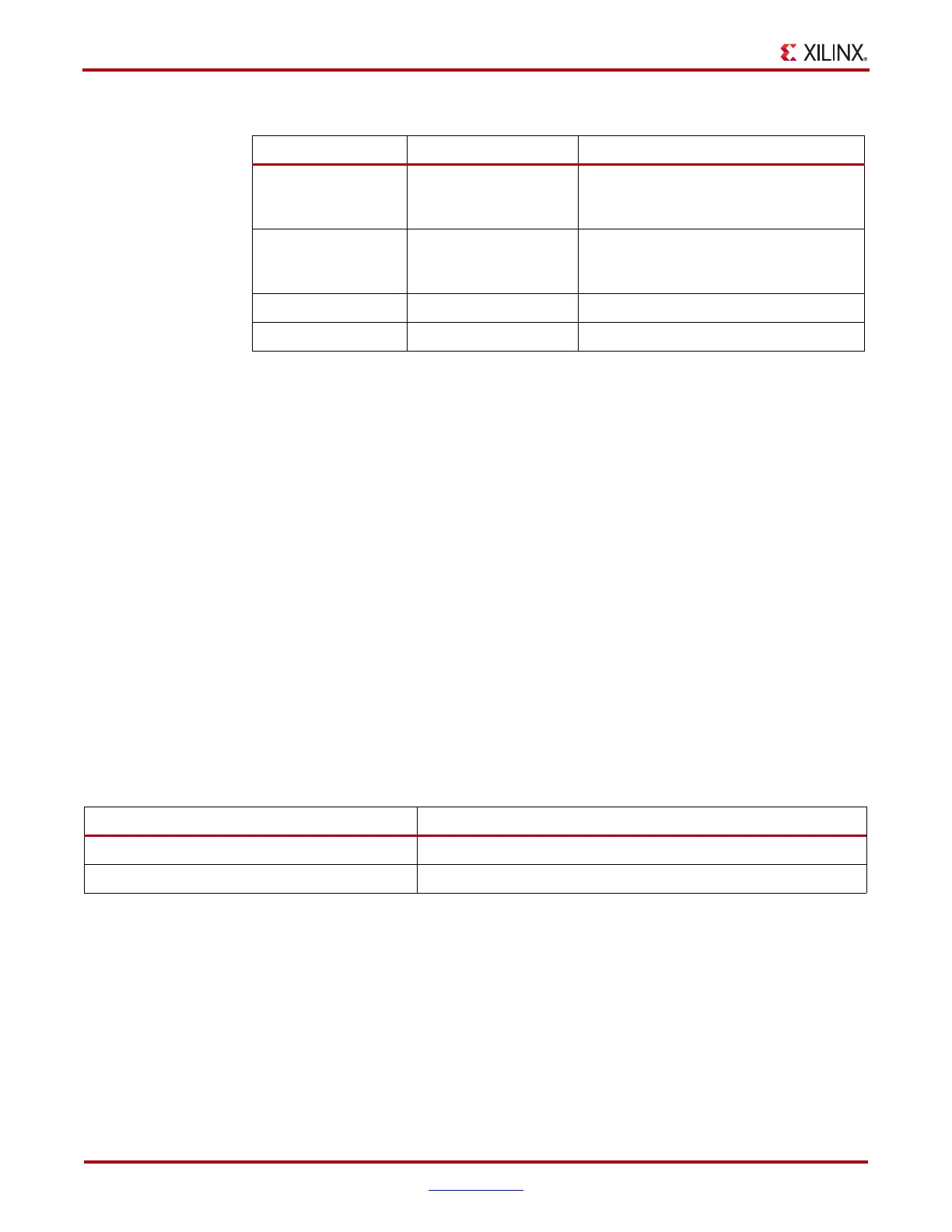
Table 2-13: Basic Power-Down Functions Summary
Function Controlled By Affects
TX PLL Power Down TXPLLPOWERDOWN The TX of the GTX transceiver. Powers
down the TX PLL as well as some of the
TX PMA circuits.
RX PLL Power Down RXPLLPOWERDOWN The RX of the GTX transceiver. Powers
down the RX PLL as well as some of the
RX PMA circuits.
TX Power Down TXPOWERDOWN[1:0] The TX of the GTX transceiver.
RX Power Down RXPOWERDOWN[1:0] The RX of the GTX transceiver.
Table 2-14: TX and RX Power States for Operation that are not for PCI Express Designs
TXPOWERDOWN[1:0] or RXPOWERDOWN[1:0] Description
00 Normal mode. The TX or RX is active sending or receiving data.
11 Power-down mode. The TX or RX is idle.

 Loading...

