158 www.xilinx.com Virtex-6 FPGA GTX Transceivers User Guide
UG366 (v2.5) January 17, 2011
Chapter 3: Transmitter
Using the TX Phase-Alignment Circuit to Bypass the Buffer
To use the TX phase-alignment circuit, follow these steps:
1. Set the following attributes with their values as follows:
a. Set TXOUTCLK_CTRL to use either TXPLLREFCLK_DIV2 or
TXPLLREFCLK_DIV1
b. Set TX_XCLK_SEL to TXUSR
c. Set TX_BUFFER_USE to FALSE
d. Set TX_PMADATA_OPT to 1’b1
2. After power-on, make sure TXPMASETPHASE and TXENPMAPHASEALIGN are
driven Low.
3. Apply GTXTXRESET and wait for TXRESETDONE to go High.
4. Drive TXENPMAPHASEALIGN High.
Keep TXENPMAPHASEALIGN High unless the phase-alignment procedure must be
repeated. Driving TXENPMAPHASEALIGN Low causes phase alignment to be lost.
5. Wait 32 TXUSRCLK2 clock cycles and then drive TXPMASETPHASE High.
6. Wait the number of required TXUSRCLK2 clock cycles as specified in Table 3-20, and
then drive TXPMASETPHASE Low. The phase of the PMACLK is now aligned with
TXUSRCLK.
The phase-alignment procedure must be redone if any of the following conditions occur:
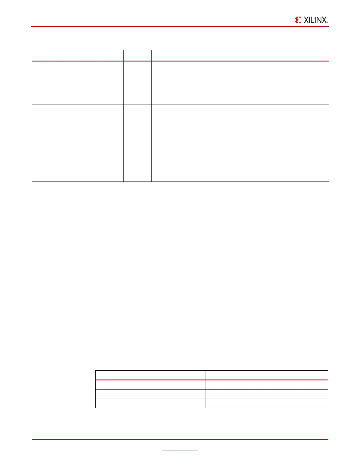
TX_XCLK_SEL String Selects the clock used to drive the clock domain in the PCS following
the TX buffer. When using the TX buffer, this attribute is set to TXOUT.
The attribute must be set as follows:
TXOUT: Use when TX_BUFFER_USE = TRUE
TXUSR: Use when TX_BUFFER_USE = FALSE
TXOUTCLK_CTRL String This attribute is the multiplexer select signal from the TX Fabric Clock
Output Control block (see Figure 3-28).
TXOUTCLKPCS (DRP value 000)
TXOUTCLKPMA_DIV1 (DRP value 001)
TXOUTCLKPMA_DIV2 (DRP value 010)
TXPLLREFCLK_DIV1 (DRP value 011)
TXPLLREFCLK_DIV2 (DRP value 100)
OFF_LOW (DRP value 101)
OFF_HIGH (DRP value 110)
Table 3-19: TX Buffer Bypass Attributes (Cont’d)
Attribute Type Description
Table 3-20: Number of Required TXUSRCLK2 Clock Cycles for Driving
TXPMASETPHASE High
TXPLL_DIVSEL_OUT TXUSRCLK2 Wait Cycles
1 8,192
2 16,384
4 32,767

 Loading...

