Virtex-6 FPGA GTX Transceivers User Guide www.xilinx.com 303
UG366 (v2.5) January 17, 2011
Appendix B
DRP Address Map of the GTX
Transceiver
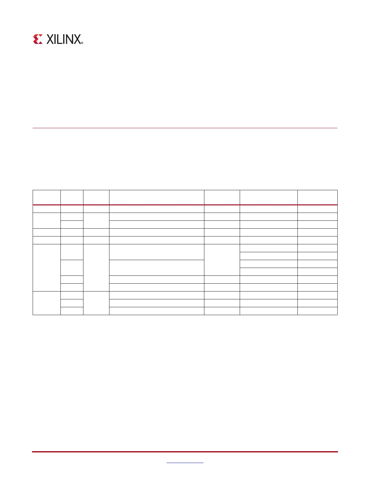
Table B-1 and Table B-2 list the DRP map sorted by address.
Note:
Do NOT modify the Reserved bits! Attributes that are not described explicitly are set
automatically by the Virtex-6 FPGA GTX Transceiver Wizard. These attributes must be left at their
defaults, except for use cases that explicitly request different values.
Table B-1: Attributes DRP Address Map
DADDR
DRP Bits R/W Attribute Name Attribute Bits Attribute Encoding
DRP Binary
Encoding
0h
15:0 R/W PMA_RX_CFG 15:0
1h
15:9
R/W
PMA_RXSYNC_CFG 6:0
8:0 PMA_RX_CFG 24:16
2h
15:0 R/W RXUSRCLK_DLY 15:0
3h
15:0 R/W BIAS_CFG 15:0
4h
15
R/W
RX_LOSS_OF_SYNC_FSM
FALSE
0
TRUE 1
14 RX_BUFFER_USE
FALSE
0
TRUE 1
13:10 CHAN_BOND_SEQ_1_ENABLE 3:0 0-15 1
(1)
9:0 CHAN_BOND_SEQ_1_1 9:0 0-1023 1
(1)
5h
15:14
R/W
Reserved 1:0
13:10 CHAN_BOND_1_MAX_SKEW 3:0 1-14
1
(1)
9:0 CHAN_BOND_SEQ_1_2 9:0 0-1023 1
(1)

 Loading...

