280 www.xilinx.com Virtex-6 FPGA GTX Transceivers User Guide
UG366 (v2.5) January 17, 2011
Chapter 5: Board Design Guidelines
Depending on availability in the package, these Quads have equal priority.
North/South Package Power Plane Prioritization
• Priority 1: MGT115
This Quad should be used if any of the GTX transceivers in the device are used in the
application. It contains the RCAL circuit that is required for the RX and TX internal
termination resistors.
• Priority 2: MGT116/117/118
If present in the Virtex-6 device, these Quads are connected in the package to the same
power planes as MGT115, the north power plane bank. Therefore they have equal
priority. Because the north power planes need to be powered for MGT115, these Quads
are also powered; therefore they can be used without additional power supply
connections.
• Priority 3: MGT110/111/112/113/114
These transceivers are connected to the south power planes. They should be used if all
Quads on the north power planes have already been utilized. If any of these Quads are
used, then all MGTAVCC_N and MGTAVTT_S pins need to be connected to the
appropriate power supply voltage.
Reference Clock
Overview
This section focuses on the selection of the reference clock source or oscillator. An oscillator
is characterized by:
•Frequency range
• Output voltage swing
• Jitter (deterministic, random, peak-to-peak)
• Rise and fall times
• Supply voltage and current
• Noise specification
• Duty cycle and duty-cycle tolerance
• Frequency stability
These characteristics are selection criteria when choosing an oscillator for a GTX
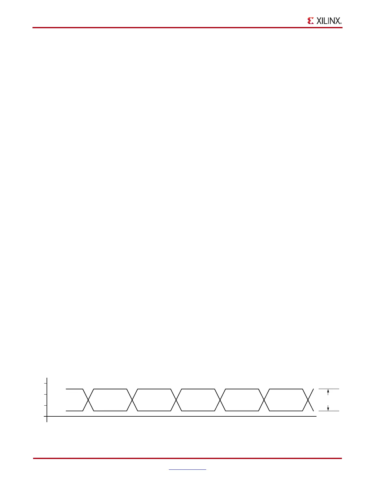
transceiver design. Figure 5-5 illustrates the convention for the single-ended clock input
voltage swing, peak- to-peak as used in the GTX transceiver portion of the Virtex-6 FPGA
Data Sheet.
X-Ref Target - Figure 5-5
Figure 5-5: Single-Ended Clock Input Voltage Swing, Peak-to-Peak
UG366_c5_05_051509
0
+ V MGTREFCLKP
MGTREFCLKN
V
ISE

 Loading...

