Virtex-6 FPGA GTX Transceivers User Guide www.xilinx.com 133
UG366 (v2.5) January 17, 2011
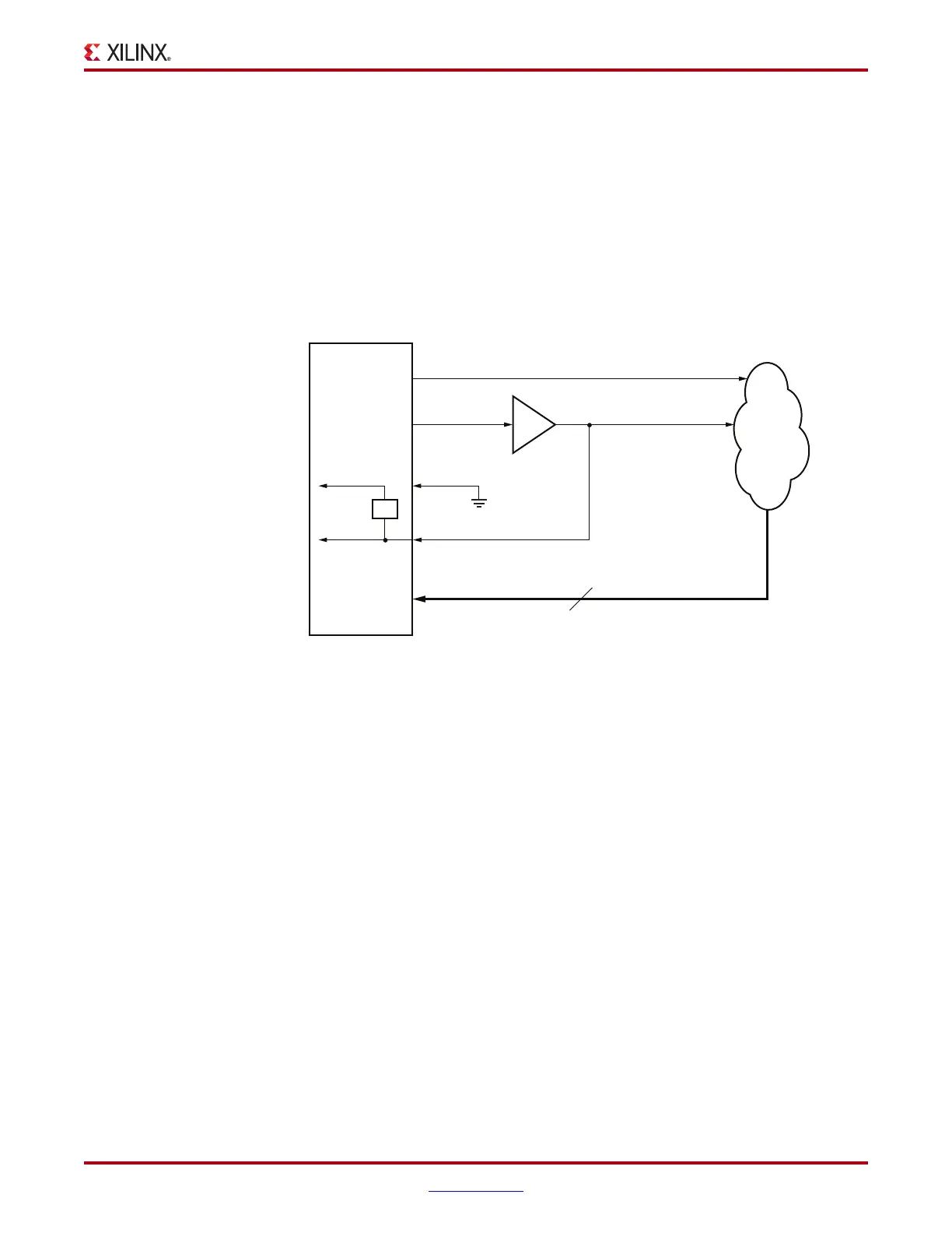
FPGA TX Interface
Refer to the Virtex-6 FPGA Data Sheet for the maximum clock frequency and jitter
limitations of BUFR. For details about placement constraints and restrictions on clocking
resources (MMCM, BUFGCTRL, IBUFDS_GTXE1, BUFG, etc.), refer to the Virtex-6 FPGA
Clocking Resources User Guide.
TXOUTCLK Driving a GTX TX in 1-Byte Mode (Single Lane)
In Figure 3-4, TXOUTCLK is used to drive TXUSRCLK2 for 1-byte mode
(TX_DATA_WIDTH = 8 or 10). The GEN_TXUSRCLK attribute is set to “TRUE”, and the
TXUSRCLK input port is tied to ground. TXUSRCLK is internally generated by dividing
TXUSRCLK2 by 2 for the internal TX PCS datapath.
Refer to the Virtex-6 FPGA Data Sheet for the maximum clock frequency and jitter
limitations of BUFR. For details about placement constraints and restrictions on clocking
resources (MMCM, BUFGCTRL, IBUFDS_GTXE1, BUFG, etc.), refer to the Virtex-6 FPGA
Clocking Resources User Guide.
TXOUTCLK Driving More Than One GTX TX in 2-Byte Mode (Multiple
Lanes)
In Figure 3-5, TXOUTCLK is used to drive multiple GTX user clocks. In this situation, the
frequency must be correct for all the GTX transceivers, and they must share the same
reference clock. In 2-byte mode (TX_DATA_WIDTH = 16 or 20), the GEN_TXUSRCLK
attribute is set to “TRUE”, and the TXUSRCLK input port is tied to ground. TXUSRCLK is
internally generated for the internal TX PCS datapath. The user can use either
TXPLLKDET or RXPLLLKDET as a reset signal for the design in the FPGA. If the TX PLL
is not used and is derived from the RX PLL, the active-High RXPLLLKDET signal should
be used instead.
X-Ref Target - Figure 3-4
Figure 3-4: TXOUTCLK Drives TXUSRCLK2 (1-Byte Mode)
GTX
Transceiver
TXPLLLKDET/
RXPLLLKDET
TXUSRCLK
Design
in
FPGA
TXUSRCLK2
TXUSRCLK
TXOUTCLK
BUFG or
BUFR
/2
TXUSRCLK2
TXDATA (8 or 10 bits)
UG366_c3_21_061609

 Loading...

