Virtex-6 FPGA GTX Transceivers User Guide www.xilinx.com 183
UG366 (v2.5) January 17, 2011
Chapter 4
Receiver
RX Overview
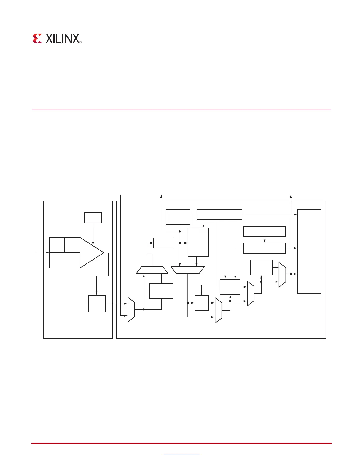
This chapter shows how to configure and use each of the functional blocks inside the GTX
receiver (RX). Each GTX transceiver includes an independent receiver, made up of a PCS
and a PMA. Figure 4-1 shows the blocks of the RX. High-speed serial data flows from
traces on the board into the PMA of the RX, into the PCS, and finally into the FPGA logic.
The key elements within the GTX RX are:
1. RX Analog Front End, page 184
2. RX Out-of-Band Signaling, page 192
3. RX Equalizer, page 194
4. RX CDR, page 204
5. RX Fabric Clock Output Control, page 207
X-Ref Target - Figure 4-1
Figure 4-1: GTX RX Block Diagram
UG366_c4_01_011111
To TX Parallel Data
(Far-End PMA Loopback)
From TX Parallel
Data (Near-End
PCS Loopback)
To T X Parallel Data
(Far-End PCS Loopback)
Polarity
RX-PMA RX-PCS
FPGA
RX
Interface
Loss of Sync
RX PIPE Control
RX Status Control
SIPO
PLL
RX
EQ
DFE
RX OOB
RX
CDR
RX
Gearbox
Over-
sampling
Elastic
Buffer
Pattern
Checker
Comma
Detect
and
Align
10B
/8B

 Loading...

