Virtex-6 FPGA GTX Transceivers User Guide www.xilinx.com 121
UG366 (v2.5) January 17, 2011
Power Down
Generic Power-Down Capabilities
The GTX transceiver provides several power-down features that can be used in a wide
variety of applications. Table 2-13 summarizes these capabilities.
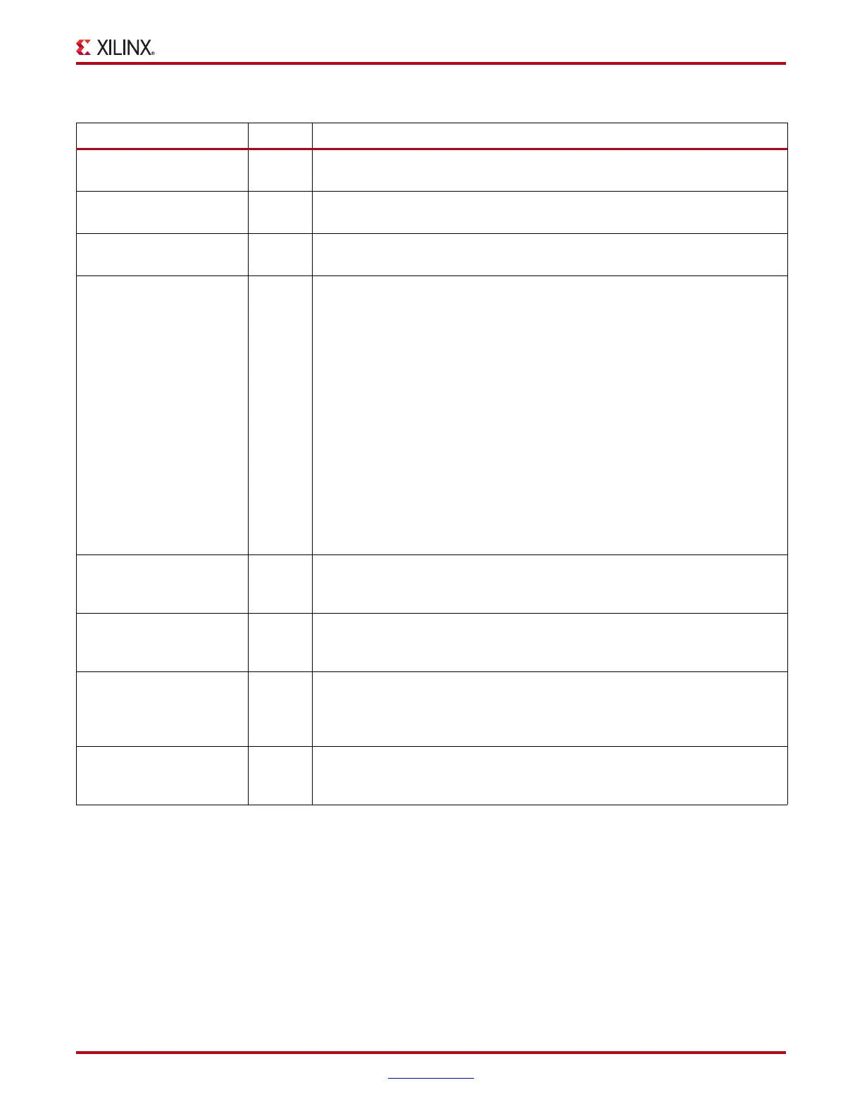
Table 2-12: Power-Down Attributes
Attribute Type Description
BGTEST_CFG 2-bit
Hex
Reserved. Use only recommended values from the Virtex-6 FPGA GTX
Transceiver Wizard.
BIAS_CFG 17-bit
Hex
Reserved. Use only recommended values from the Virtex-6 FPGA GTX
Transceiver Wizard.
PMA_TX_CFG 20-bit
Hex
Reserved. Use only recommended values from the Virtex-6 FPGA GTX
Transceiver Wizard.
POWER_SAVE 10-bit
Binary
POWER_SAVE[4]:
Mux select for the TXOUTCLK output clock. Must be tied to 1’b1.
1'b0: Use the TX Delay Aligner
1'b1: Bypass the TX Delay Aligner
POWER_SAVE[5]:
Mux select for the RXRECCLK output clock. Must be tied to 1’b1 when RX
buffer is used (RX_BUFFER_USE = TRUE). When RX buffer is bypassed, refer
to Using the RX Phase Alignment Circuit to Bypass the Buffer, page 235.
1'b0: Use the RX Delay Aligner
1'b1: Bypass the RX Delay Aligner
All other bits are reserved. Use recommended values from the Virtex-6 FPGA
GTX Transceiver Wizard.
TRANS_TIME_FROM_P2 12-bit
Hex
Counter settings for programmable transition time from P2 state for PCIe
operation. Use recommended values from the Virtex-6 FPGA GTX Transceiver
Wizard.
TRANS_TIME_NON_P2 8-bit
Hex
Counter settings for programmable transition time to/from all states except P2
for PCIe operation. Use recommended values from the Virtex-6 FPGA GTX
Transceiver Wizard.
TRANS_TIME_RATE 8-bit
Hex
Counter settings for programmable transition time when rate is changed using
RATE pins for all protocols including the PCIe protocol (Gen2/Gen1 data
rates). Set to the maximum value for non PCIe modes. Use recommended
values from the Virtex-6 FPGA GTX Transceiver Wizard.
TRANS_TIME_TO_P2 10-bit
Hex
Counter settings for programmable transition time to the P2 state for PCIe
operation. Use recommended values from the Virtex-6 FPGA GTX Transceiver
Wizard.

 Loading...

