Virtex-6 FPGA GTX Transceivers User Guide www.xilinx.com 197
UG366 (v2.5) January 17, 2011
RX Equalizer
Ports and Attributes
Table 4-11 defines the RX equalizer ports.
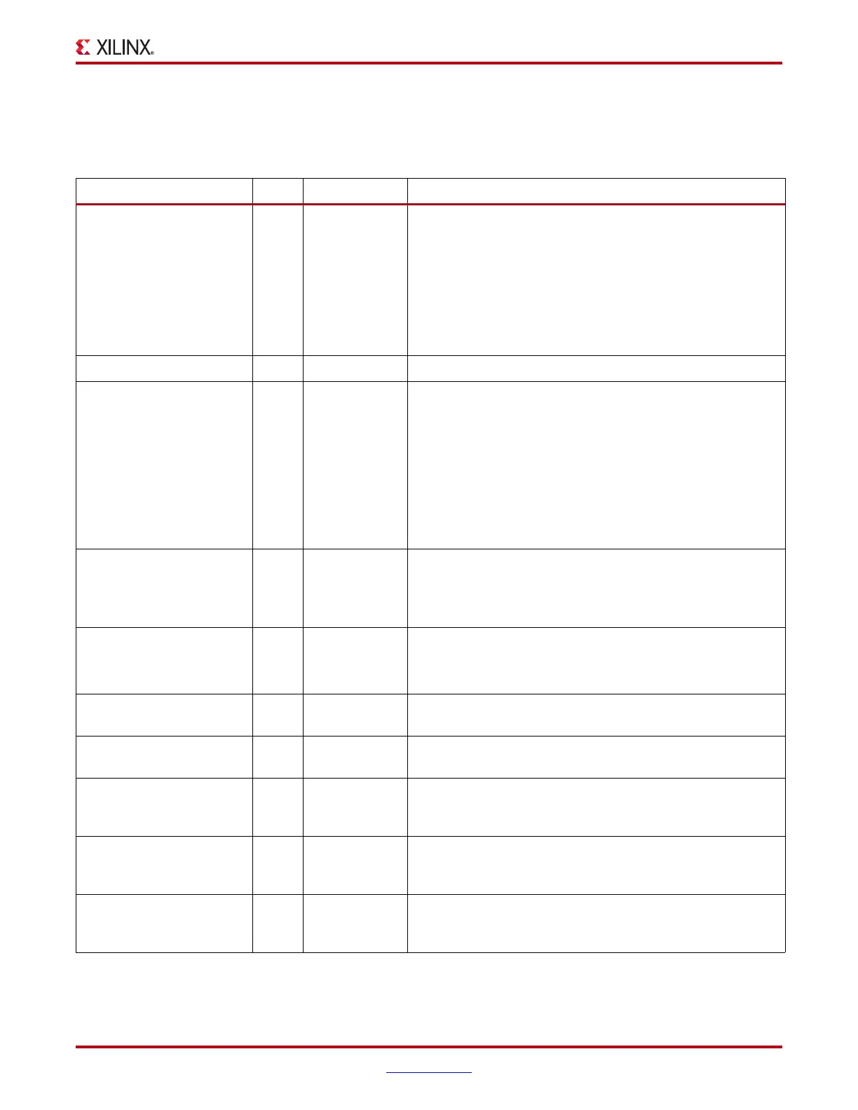
Table 4-11: RX Equalizer Ports
Port Dir Clock Domain Description
DFECLKDLYADJ[5:0] In RXUSRCLK2 DFE clock delay adjust override for each transceiver.
000000: Phase difference between the bit serial sample
clock and the DFECLK is 0°.
111111: Phase difference between the bit serial sample
clock and the DFECLK is 90°.
This DFE is automatically calibrated for optimal performance
by a built-in state machine. This override value is only
accepted when DFEDLYOVRD is 1.
DFECLKDLYADJMON[5:0] Out RXUSRCLK2 DFE clock delay calibration result monitor for each transceiver.
DFEDLYOVRD In RXUSRCLK2 Override enable for the DFE clock delay adjustment.
0: Use the optimized DFE clock delay calibration value
(recommended).
1: Override the DFE clock delay calibration state machine
with the value provided by DFECLKDLYADJ[5:0]. The
optimized DFE clock delay calibration is done when
GTXRXRESET is deasserted.
When switching from override mode to the optimized mode
dynamically, always toggle GTXRXRESET.
DFEEYEDACMON[4:0] Out RXUSRCLK2 Averaged Vertical Eye Height (voltage domain) used by the
DFE as an optimization criterion.
11111: Indicates approximately 200 mV
PPD
of internal eye
opening.
DFESENSCAL[2:0] Out RXUSRCLK2 Sampler sensitivity self-calibration after the reset.
000: Lowest offset
111: Highest offset
DFETAP1[4:0] In RXUSRCLK2 DFE tap 1 weight value control for each transceiver (5-bit
resolution).
DFETAP1MONITOR[4:0] Out RXUSRCLK2 DFE tap 1 weight value monitor for each transceiver (5-bit
resolution).
DFETAP2[4:0] In RXUSRCLK2 DFE tap 2 weight value control for each transceiver (4-bit
resolution plus 1-bit sign). For example, –2 is represented as
1 0010.
DFETAP2MONITOR[4:0] Out RXUSRCLK2 DFE tap 2 weight value monitor for each transceiver (4-bit
resolution plus 1-bit sign). For example, –2 is represented as
1 0010.
DFETAP3[3:0] In RXUSRCLK2 DFE tap 3 weight value control for each transceiver (3-bit
resolution plus 1-bit sign). For example, –2 is represented as
1 010.

 Loading...

