170 www.xilinx.com Virtex-6 FPGA GTX Transceivers User Guide
UG366 (v2.5) January 17, 2011
Chapter 3: Transmitter
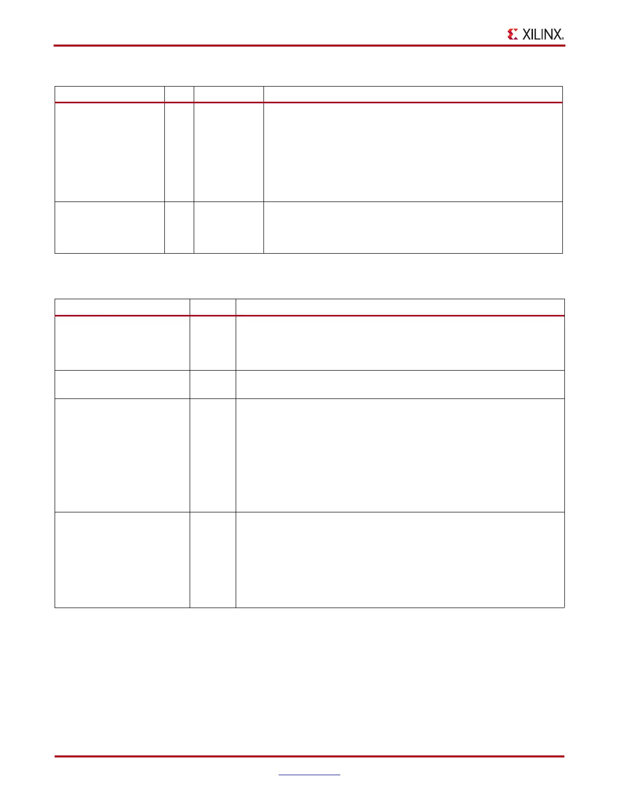
Table 3-30 defines the TX Fabric Clock Output Control block attributes.
PCI Express Clocking Use Mode
In most applications, TXOUTCLK port is used to clock the FPGA logic. TXOUTCLKPCS
via TXOUTCLK is used for the oversampling mode, and TXPLLREFCLK via TXOUTCLK
is used for the rest of the applications.
For PCI Express clocking, the use case is to route the reference clock from IBUFDS_GTXE1
directly to the FPGA user logic instead of through TXOUTCLK if the TX buffer is used, as
shown in Figure 3-29. However, if TX buffer is bypassed and compensation for voltage
TXRATE In TXUSRCLK2 This port controls the setting for the TX serial clock divider for low
line rate support (see Table 3-28). This input port is used in
combination with the TXPLL_DIVSEL_OUT attribute.
00: Let TXPLL_DIVSEL_OUT determine the D divider value
01: Set D divider to 4
10: Set D divider to 2
11: Set D divider to 1
TXRATEDONE Out TXUSRCLK2 The TXRATEDONE port is asserted High for one TXUSRCLK2 cycle
in response to a change on the TXRATE port. The
TRANS_TIME_RATE attribute defines the period of time between a
change on the TXRATE port and the assertion of TXRATEDONE.
Table 3-29: TX Fabric Clock Output Control Ports (Cont’d)
Port Dir Clock Domain Description
Table 3-30: TX Fabric Clock Output Control Attributes
Attribute Type Description
TRANS_TIME_RATE 8-bit
Hex
Reserved. Use only recommended values from the Virtex-6 FPGA GTX
Transceiver Wizard.
This attribute determines when PHYSTATUS and TXRATEDONE are
asserted after a rate change.
TX_EN_RATE_RESET_BUF Boolean When set to TRUE, this attribute enables automatic TX buffer reset during a
rate change event initiated by a change in TXRATE.
TXOUTCLK_CTRL String This attribute is the multiplexer select signal in Figure 3-28, page 167. It
determines which GTX transceiver internal clock is output to the FPGA logic
via the TXOUTCLK port. Valid settings are:
“TXOUTCLKPCS”
“TXOUTCLKPMA_DIV1”
“TXOUTCLKPMA_DIV2”
“TXPLLREFCLK_DIV1”
“TXPLLREFCLK_DIV2”
TXPLL_DIVSEL_OUT Integer This attribute controls the setting for the TX serial clock divider for low line
rate support (see Table 3-28, page 168). This attribute is only valid when
TXRATE = 00. Otherwise the D divider value is controlled by TXRATE.
Valid settings are:
1: Set the D divider to 1
2: Set the D divider to 2
4: Set the D divider to 4

 Loading...

