208 www.xilinx.com Virtex-6 FPGA GTX Transceivers User Guide
UG366 (v2.5) January 17, 2011
Chapter 4: Receiver
Serial Clock Divider
Each receiver PMA module has a D divider that divides down the clock from the PLL for
lower line rate support. This divider can be set statically for applications with a fixed line
rate or it can be changed dynamically for protocols with multiple line rates.
To use the D divider in fixed line rate applications, the RXPLL_DIVSEL_OUT attribute
must be set to the appropriate value, and the RXRATE[1:0] port needs to be tied to 00.
To use the D divider in multiple line rate applications, the RXRATE[1:0] port is used to
dynamically select the D divider value. The RXPLL_DIVSEL_OUT attribute and the
RXRATE[1:0] port must select the same D divider value upon device configuration. After
device configuration, the RXRATE[1:0] is used to dynamically change the D divider value.
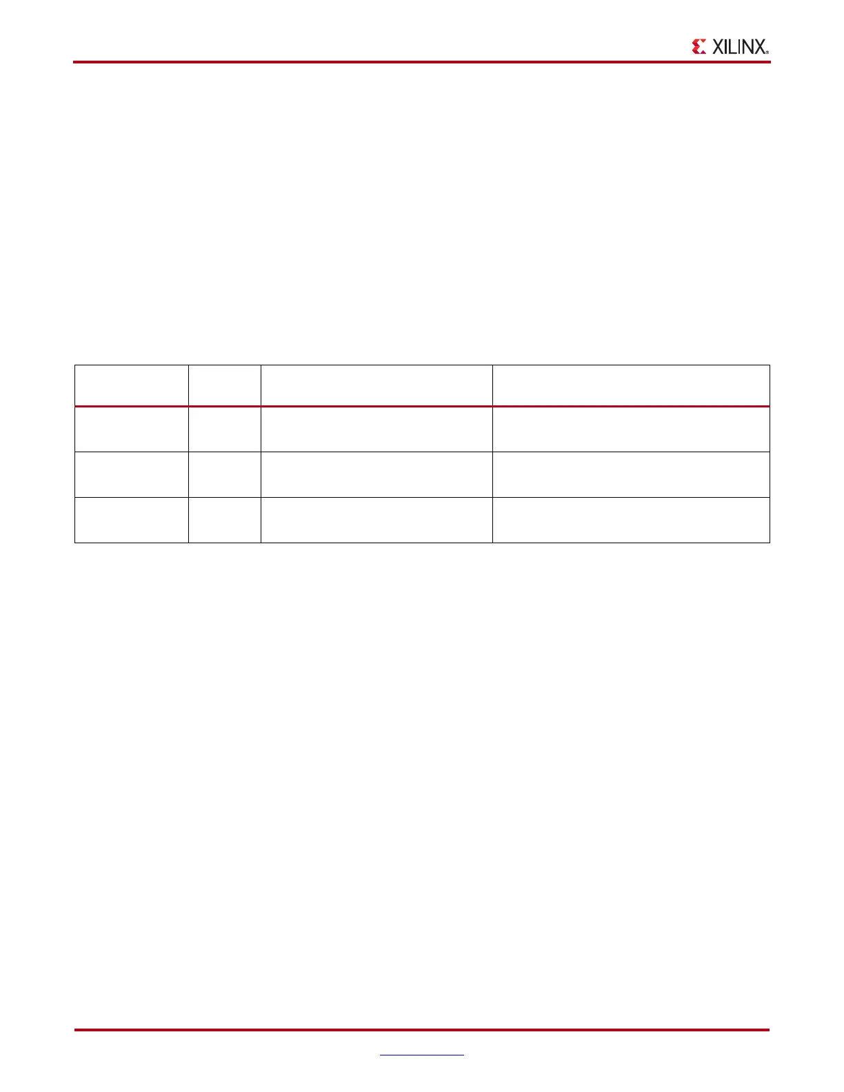
The control for the serial divider is described in Table 4-23. For details about the line rate
range per speed grade, refer to the Virtex-6 FPGA Data Sheet.
Parallel Clock Divider and Selector
The recovered clock can be brought out to the FPGA logic. The recovered clock is used by
protocols that do not have a clock compensation mechanism and require to use a clock
synchronous to the data, the recovered clock, to clock the downstream fabric logic. The
parallel clock divider block can output a 1-byte or 2-byte data width recovered clock.
When the recovered clock is needed, the recommended clock output is RXRECCLK. The
attribute RXRECCLK_CTRL controls the input selector and allows the following clocks to
be output via RXRECCLK port:
• RXRECCLKPCS: This clock should only be used when the RX Oversampling block is
enabled. The RX Oversampling block divides down the RXRECCLKPMA_DIV2 clock
to match the 5X oversampled data rate.
• RXRECCLKPMA_DIV1/DIV2: This is the recovered clock after the CDR and is used
when the RX Oversampling block is not used.
• RXPLLREFCLK_DIV1/DIV2: This is the input reference clock to the RX PLL and is
typically not used. For usages that do not require outputting a recovered clock to the
fabric, RXPLLREFCLK_DIV1/DIV2 can be used as the system clock. However,
TXOUTCLK is usually used as system clock.
The RXRECCLKPMA_DIV2 output is the 2-byte datapath frequency and is used when
RXDATA is 2 bytes. The RXRECCLKPMA_DIV1 output is the 1-byte datapath frequency
and is used when RXDATA is 1 byte.
RXRECCLK output has an output delay control used for applications that bypass the RX
buffer for constant datapath delay. Refer to RX Buffer Bypass, page 231 for more details.
Table 4-23: RX PLL Output Divider Setting
Line Rate Range
(Gb/s)
D Divider
Value
Static Setting via Attribute Dynamic Control via Ports
2.40 to 6.60 1 RXPLL_DIVSEL_OUT = 1
RXRATE[1:0] = 00
RXRATE[1:0] = 11
1.20 to 3.3 2 RXPLL_DIVSEL_OUT = 2
RXRATE[1:0] = 00
RXRATE[1:0] = 10
0.60 to 1.65 4 RXPLL_DIVSEL_OUT = 4
RXRATE[1:0] = 00
RXRATE[1:0] = 01

 Loading...

