Virtex-6 FPGA GTX Transceivers User Guide www.xilinx.com 171
UG366 (v2.5) January 17, 2011
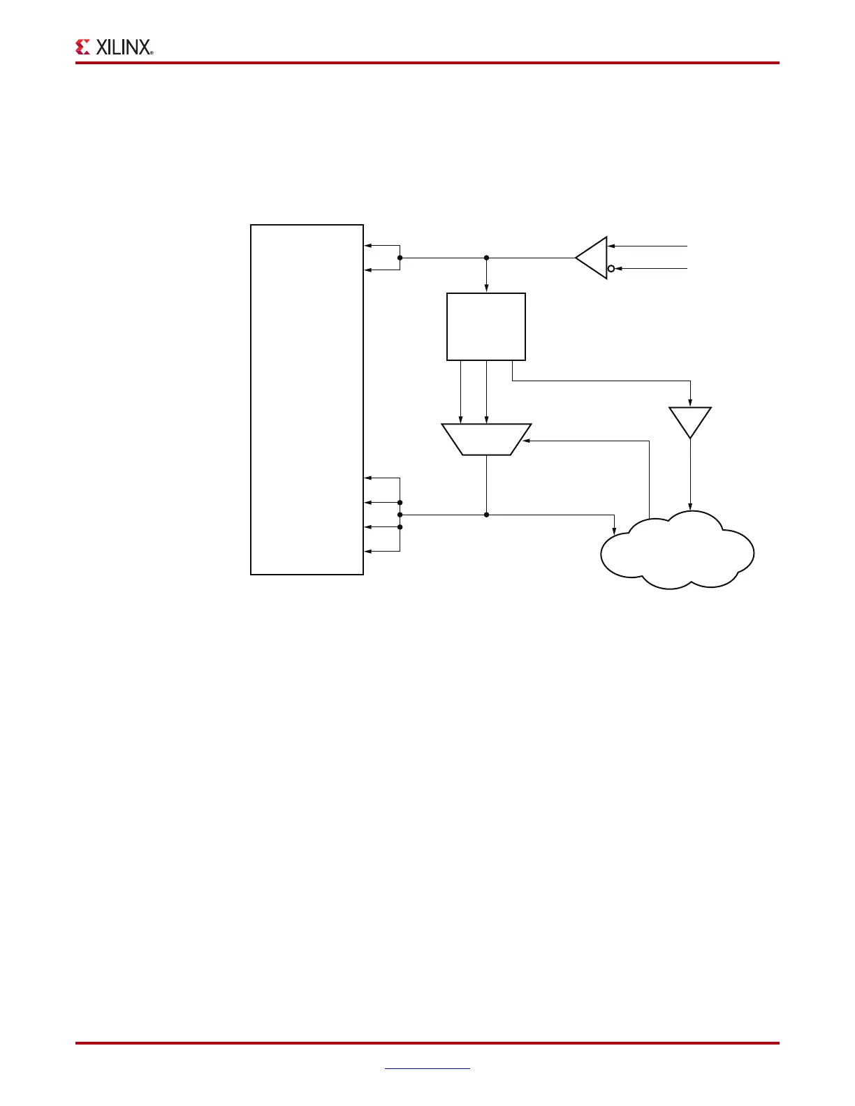
TX Fabric Clock Output Control
and/or temperature variations from the global clock trees is necessary, TXOUTCLK must
be used as the user clock source. See TX Buffer Bypass, page 155 for more details. In
Figure 3-29, TXRATE_SEL is an FPGA user logic control signal that selects a new PCLK
frequency from the BUFGMUX (125 MHz or 250 MHz) for a rate change. PCLK is the PIPE
clock for the FPGA user logic and is the parallel interface clock used to synchronize data
transfers across the parallel interface.
Note:
The IBUFDS_GTXE1 diagram in Figure 3-29 is a simplification. The output port ODIV2 is left
floating, and the input port CEB is set to logic 0.
For details about placement constraints and restrictions on clocking resources (MMCM,
BUFGCTRL, IBUFDS_GTXE1, BUFG, etc.), refer to the Virtex-6 FPGA Clocking Resources
User Guide.
Rate Change Use Mode for PCI Express 2.0 Operation
In PCI Express mode, TXRATE[1] must be tied to 1, and TXRATE[0] is used for line rate
change. RXRATE[1:0] must be tied to TXRATE[1:0]. The TXPLL_DIVSEL_OUT attribute
must be set to 2.
To perform a PCI Express line rate change, TXPOWERDOWN must be in the P0 power
state, and TXELECIDLE must be asserted. A change in TXRATE[0] initiates a PCI Express
line rate change. If an MMCM is used to generate the 125 MHz and 250 MHz user clocks,
a BUFGMUX is recommended to be used. The TXRATEDONE single cycle pulse can be
used as an timing indicator to change the clock frequency from BUFGMUX. The
PHYSTATUS single cycle pulse indicates that the PCI Express line rate change is
completed.
X-Ref Target - Figure 3-29
Figure 3-29: PCI Express Clocking
GTX
Transceiver
FPGA
User Logic
REF_CLKP
125 MHz
250 MHz
SYS_CLK
TXRATE_SEL
REF_CLKN
IBUFDS_GTXE1
BUFG
BUFGMUX
PCLK
MGTREFCLKTX
MGTREFCLKRX
TXUSRCLK
TXUSRCLK2
RXUSRCLK
RXUSRCLK2
MMCM
UG366_c3_31_122209

 Loading...

