EasyManua.ls Logo

Xilinx Virtex-6 FPGA User Manual

Xilinx Virtex-6 FPGA
317 pages
To Next Page IconTo Next Page
To Previous Page IconTo Previous Page
Page #226 background imageLoading...
Page #226 background image
226 www.xilinx.com Virtex-6 FPGA GTX Transceivers User Guide
UG366 (v2.5) January 17, 2011
Chapter 4: Receiver
RX Loss-of-Sync State Machine
Functional Description
Several 8B/10B protocols make use of a standard Loss-of-Sync (LOS) state machine to
detect when the channel is malfunctioning. Each GTX receiver includes a LOS state
machine that can be activated for protocols requiring it. When the state machine is not
used, the LOS state machine's ports can be re-used to monitor the condition of incoming
data.
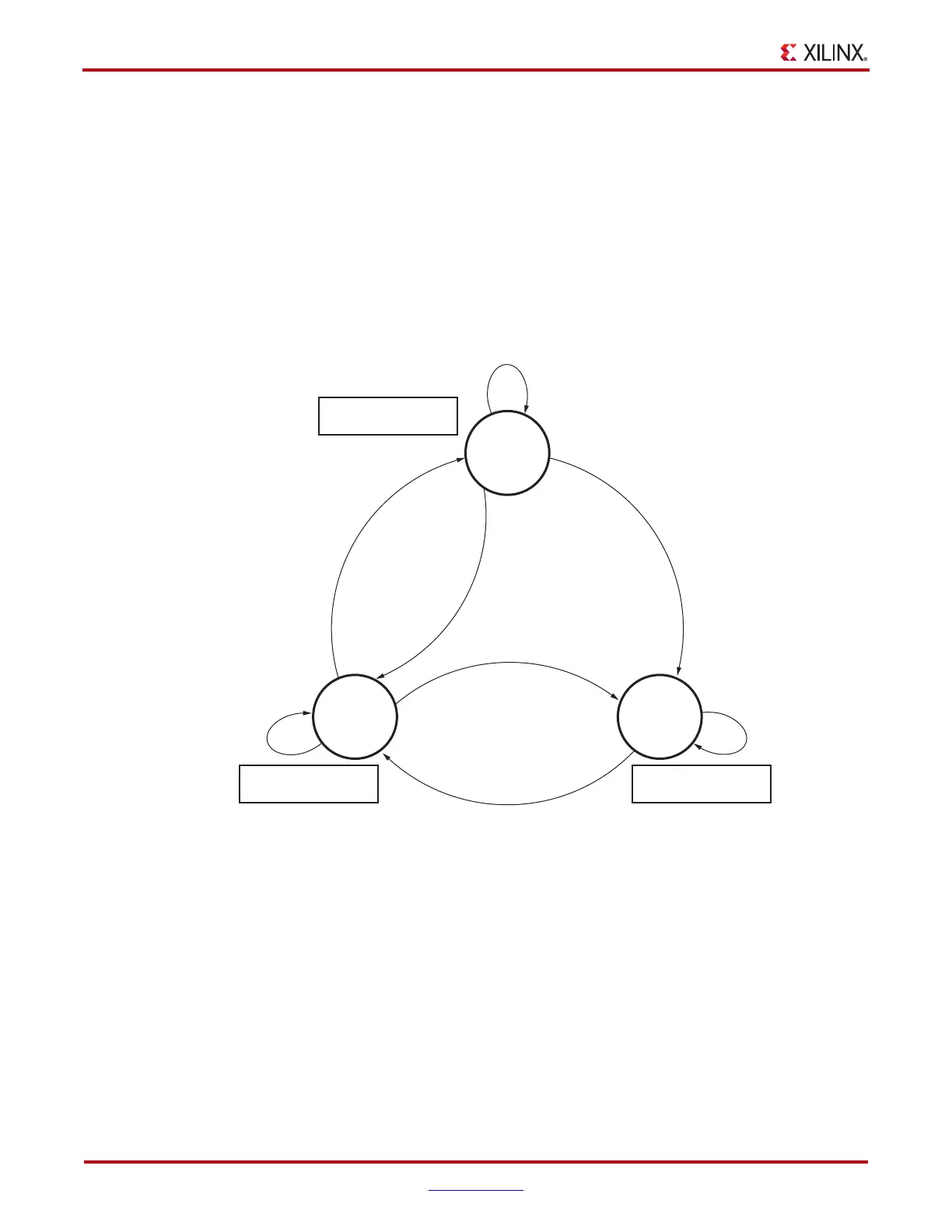
Figure 4-28 shows the standard LOS state machine, used in several 8B/10B protocols (for
example, XAUI) to detect problems in the incoming data stream.
To activate the LOS state machine in the GTX transceiver, RX_LOSS_OF_SYNC_FSM is set
to TRUE. While the state machine is active, the RXLOSSOFSYNC port presents its current
state.
If the LOS state machine is inactive (RX_LOSS_OF_SYNC_FSM = FALSE), the
RXLOSSOFSYNC port presents information about the received data. The
RXLOSSOFSYNC entry in Table 4-36 shows the meaning of the RXLOSSOFSYNC port in
this case.
The operation of the LOS state machine can be tuned using the RX_LOS_INVALID_INCR
and RX_LOS_THRESHOLD attributes. RX_LOS_THRESHOLD adjusts how sensitive the
LOS state machine is to bad characters (RX_LOS_THRESHOLD divided by
RX_LOS_INVALID_INCR) to change the machine from the SYNC_ACQUIRED state to the
X-Ref Target - Figure 4-28
Figure 4-28: LOS State Machine
00
01 10
No Comma Received
Count = RX_LOS_THRESHOLD
Count < RX_LOS_THRESHOLD/RX_LOS_INVALID_INCR
Channel Alignment
or
Comma Realignment
Invalid Data
Comma Received
UG366_c4_25_102910
Valid Data + 4 RXRECCLK Cycles
Valid Data + < 4 RXRECCLK Cycles
SYNC_ACQUIRED
RESYNC LOSS_OF_SYNC
www.BDTIC.com/XILINX

Table of Contents

Other manuals for Xilinx Virtex-6 FPGA

Question and Answer IconNeed help?

Do you have a question about the Xilinx Virtex-6 FPGA and is the answer not in the manual?

Xilinx Virtex-6 FPGA Specifications

General IconGeneral
Technology40nm
Clock Data Recovery (CDR)Integrated
Logic CellsUp to 760, 000
I/O PinsUp to 1200
Transceiver FeaturesPre-emphasis, equalization
Transceiver Protocol SupportPCIe, SATA, Ethernet, CPRI, OBSAI, Serial RapidIO
Power ConsumptionVaries by model and configuration
Transceiver TypeMulti-Gigabit Transceivers (RocketIO GTP/GTX)

Summary

Preface: About This Guide

Guide Contents

Lists the chapters and appendices included in this manual.

Additional Documentation

Provides links to other Xilinx documents for further information.

Chapter 1: Transceiver and Tool Overview

Overview

Introduces the Virtex-6 FPGA GTX transceiver and its features.

Port and Attribute Summary

Summarizes GTX ports and attributes, grouped by functionality.

Simulation

Explains prerequisites and setup for simulating GTX transceiver designs.

Implementation

Details mapping GTX transceivers to device resources and UCF creation.

Chapter 2: Shared Transceiver Features

Reference Clock Input Structure

Describes the structure and ports for reference clock inputs.

Reference Clock Selection

Explains how to select and route reference clocks for GTX transceivers.

PLL

Details the Phase-Locked Loop (PLL) architecture and its settings.

Power Down

Describes the various power-down modes and capabilities of the GTX transceiver.

Loopback

Explains loopback modes for testing the transceiver datapath.

ACJTAG

Covers the ACJTAG interface support for GTX transceivers.

Dynamic Reconfiguration Port

Explains the DRP for dynamic parameter changes in GTXE1 primitive.

Chapter 3: Transmitter

TX Overview

Introduces the functional blocks and key elements of the GTX transmitter.

FPGA TX Interface

Describes the gateway for transmitting data to the GTX transceiver.

TX Initialization

Details the procedures for resetting and initializing the GTX TX.

TX 8B/10B Encoder

Explains the 8B/10B encoding scheme used for outgoing data.

TX Gearbox

Describes support for 64B/66B and 64B/67B encoding for high-speed protocols.

TX Buffer

Explains the TX buffer's role in resolving phase differences between domains.

TX Buffer Bypass

Covers the advanced feature of bypassing the TX buffer for reduced latency.

TX Pattern Generator

Details the PRBS and other patterns for testing signal integrity.

TX Oversampling

Explains the built-in 5X oversampling feature for serial rates.

TX Polarity Control

Describes the function to invert outgoing data polarity before transmission.

TX Fabric Clock Output Control

Details the serial and parallel clock divider control for TX fabric clocks.

TX Configurable Driver

Explains the high-speed current-mode differential output buffer features.

TX Receiver Detect Support for PCI Express Designs

Describes the feature for detecting receiver presence on a link.

TX Out-of-Band Signaling

Covers support for SATA/SAS OOB sequences and PCI Express beaconing.

Chapter 4: Receiver

RX Overview

Introduces the functional blocks and key elements of the GTX receiver.

RX Analog Front End

Describes the high-speed current-mode input differential buffer.

RX Out-of-Band Signaling

Covers support for decoding SATA/SAS OOB sequences and PCI Express beacons.

RX Equalizer

Explains the circuit for compensating high-frequency losses in the channel.

RX CDR

Details the Clock Data Recovery circuit for extracting clock and data.

RX Fabric Clock Output Control

Covers serial and parallel clock divider control for RX fabric clocks.

RX Margin Analysis

Discusses methods for determining link quality via eye diagrams.

RX Polarity Control

Describes the function to invert incoming data polarity.

RX Oversampling

Explains the built-in 5X oversampling for low serial rates.

RX Pattern Checker

Details the built-in PRBS checker for testing channel signal integrity.

RX Byte and Word Alignment

Explains the process of aligning serial data to byte boundaries.

RX Loss-of-Sync State Machine

Describes the state machine for detecting channel malfunction.

RX 8B/10B Decoder

Explains the decoder for RX data, indicating errors and control sequences.

RX Buffer Bypass

Covers the advanced feature of bypassing the RX elastic buffer for low latency.

RX Elastic Buffer

Explains the buffer for resolving clock domain differences.

RX Clock Correction

Details the circuit for tolerating frequency differences between clock domains.

RX Channel Bonding

Describes using the RX elastic buffer to cancel skew between lanes.

RX Gearbox

Describes support for 64B/66B and 64B/67B encoding for high-speed protocols.

RX Initialization

Details the procedures for resetting and initializing the GTX RX.

FPGA RX Interface

Describes the interface for receiving RX data from the GTX RX.

Chapter 5: Board Design Guidelines

Overview

Discusses implementing GTX transceivers on a PCB for optimal performance.

Pin Description and Design Guidelines

Describes GTX transceiver pins and provides design guidelines.

Termination Resistor Calibration Circuit

Explains the circuit for calibrating termination resistors.

Analog Power Supply Pins

Details the MGTAVCC and MGTAVTT analog power supply pins.

Reference Clock

Focuses on the selection criteria for reference clock sources.

Power Supply Distribution Network

Discusses issues regarding power supply implementation on the PCB.

Crosstalk

Explains how crosstalk degrades GTX transceiver performance and how to avoid it.

SelectIO Usage Guidelines

Provides guidelines for SelectIO interface usage to minimize GTX impact.

Related product manuals