Virtex-6 FPGA GTX Transceivers User Guide www.xilinx.com 23
UG366 (v2.5) January 17, 2011
Port and Attribute Summary
This cluster of four GTX transceivers share two differential reference clock pin pairs and
clock routing. Chapter 2, Shared Transceiver Features, discusses details about reference
clock sources and the routing.
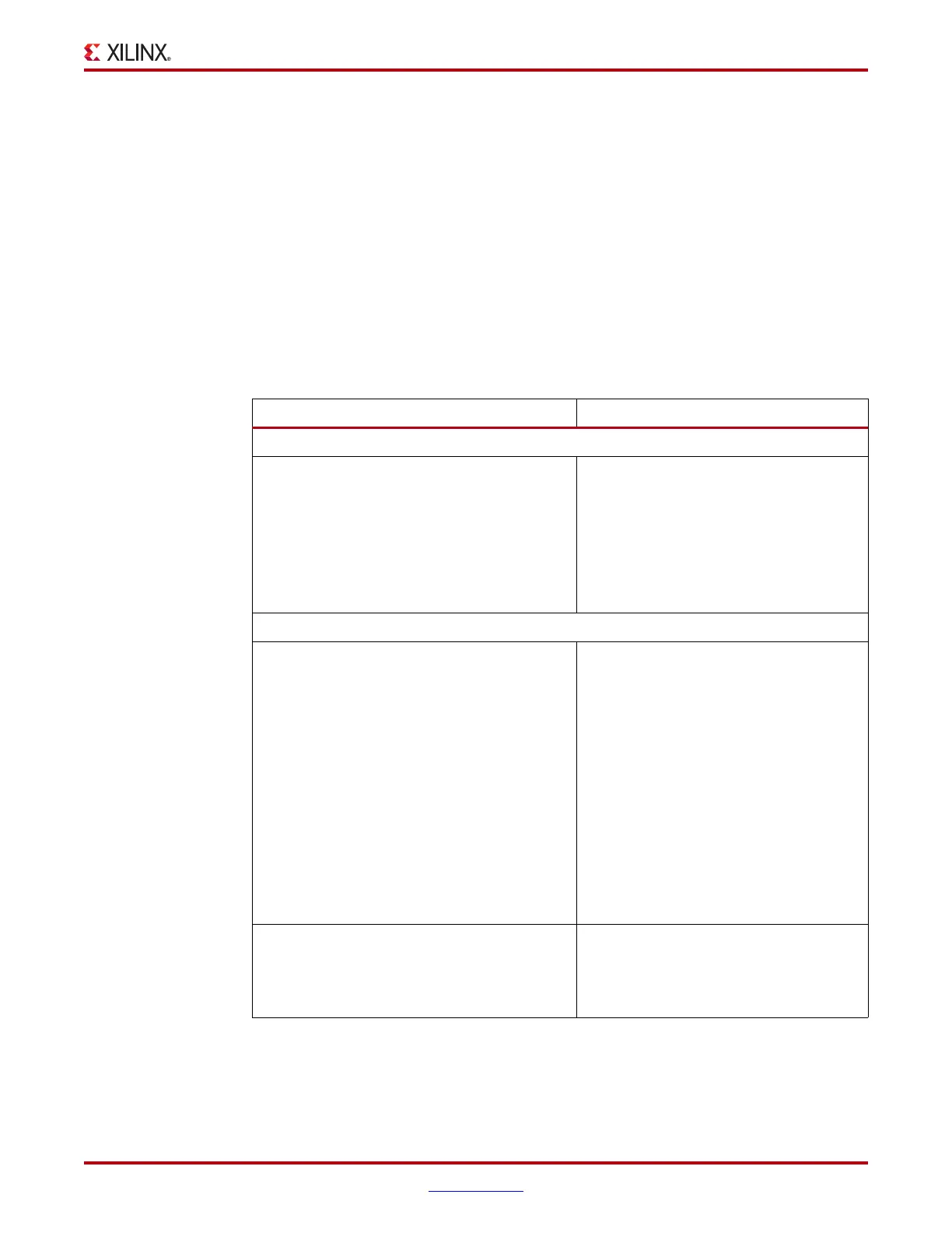
Port and Attribute Summary
The ports and attributes are grouped in tables for each functionality group (e.g., reference
clock selection). If a port or attribute appears in multiple chapters, it is listed in the group
of its first appearance. Table 1-1 summarizes the ports and attributes according to
functionality group.
Note:
Ta bl e 1 -1 lists all the ports and attributes covered in this user guide. Some ports or attributes
are present in the instantiation primitive or are listed in Appendix B, DRP Address Map of the GTX
Transceiver but not in Tabl e 1 -1 .
Table 1-1: Port and Attribute Summary
Port/Attribute Section, Page
Simulation
Attributes:
• SIM_GTXRESET_SPEEDUP
• SIM_RECEIVER_DETECT_PASS
• SIM_RXREFCLK_SOURCE
• SIM_TX_ELEC_IDLE_LEVEL
• SIM_TXREFCLK_SOURCE
• SIM_VERSION
page 38
page 38
page 39
page 39
page 39
page 39
Clocking
Ports:
• GREFCLKRX
• GREFCLKTX
• MGTREFCLKRX[1:0]
• MGTREFCLKTX[1:0]
• NORTHREFCLKRX[1:0]
• NORTHREFCLKTX[1:0]
• PERFCLKRX
• PERFCLKTX
• RXPLLREFSELDY[2:0]
• SOUTHREFCLKRX[1:0]
• SOUTHREFCLKTX[1:0]
• TXPLLREFSELDY[2:0]
page 106
page 106
page 106
page 106
page 106
page 106
page 106
page 106
page 107
page 107
page 107
page 107
Attributes:
• PMA_CAS_CLK_EN
• SIM_RXREFCLK_SOURCE[2:0]
• SIM_TXREFCLK_SOURCE[2:0]
page 107
page 107
page 107

 Loading...

