Virtex-6 FPGA GTX Transceivers User Guide www.xilinx.com 155
UG366 (v2.5) January 17, 2011
TX Buffer Bypass
TX Buffer Bypass
Functional Description
Bypassing the TX buffer is an advanced feature of the Virtex-6 FPGA GTX transceivers. The
TX phase-alignment circuit is used to adjust the phase difference between the PMA
parallel clock domain (XCLK) and the TXUSRCLK domain when the TX buffer is
bypassed. Figure 3-20, page 153 shows the XCLK and USRCLK domains. Table 3-15,
page 153 shows the trade-offs between the buffer and the buffer bypass modes.
The system margin in TX Buffer Bypass mode depends on the TXUSRCLK frequency and
the model. To enhance the system margin for better compensation to temperature and/or
voltage variation, additional requirements on the clocking use model must be met. These
requirements are described in the section Transmit Fabric Clocking Use Model for TX
Buffer Bypass, page 161.
To ensure that the TXOUTCLK output port operates at the desired frequency in TX buffer
bypass mode, all of the following conditions must be met:
• When the TX PLL supplies the clock for the TX datapath (TX_CLK_SOURCE =
“TXPLL”):
• The transmitter reference clock must always be toggling
• TXPLLPOWERDOWN must be tied Low
• When the RX PLL supplies the clock for the TX datapath (TX_CLK_SOURCE =
“RXPLL”):
• The receiver reference clock must always be toggling
• RXPLLPOWERDOWN must be tied Low
• GTXTXRESET, GTXRXRESET, PLLTXRESET, and PLLRXRESET must not be tied
High.
For transceivers that are not instantiated in the user design, the ISE® software, version 12.1
or later, automatically ensures that the TXOUTCLK performance is preserved for future
use. MGTAVCC must be supplied to these transceivers. Refer to Managing Unused GTX
Transceivers, page 276 for more information.
Ports and Attributes
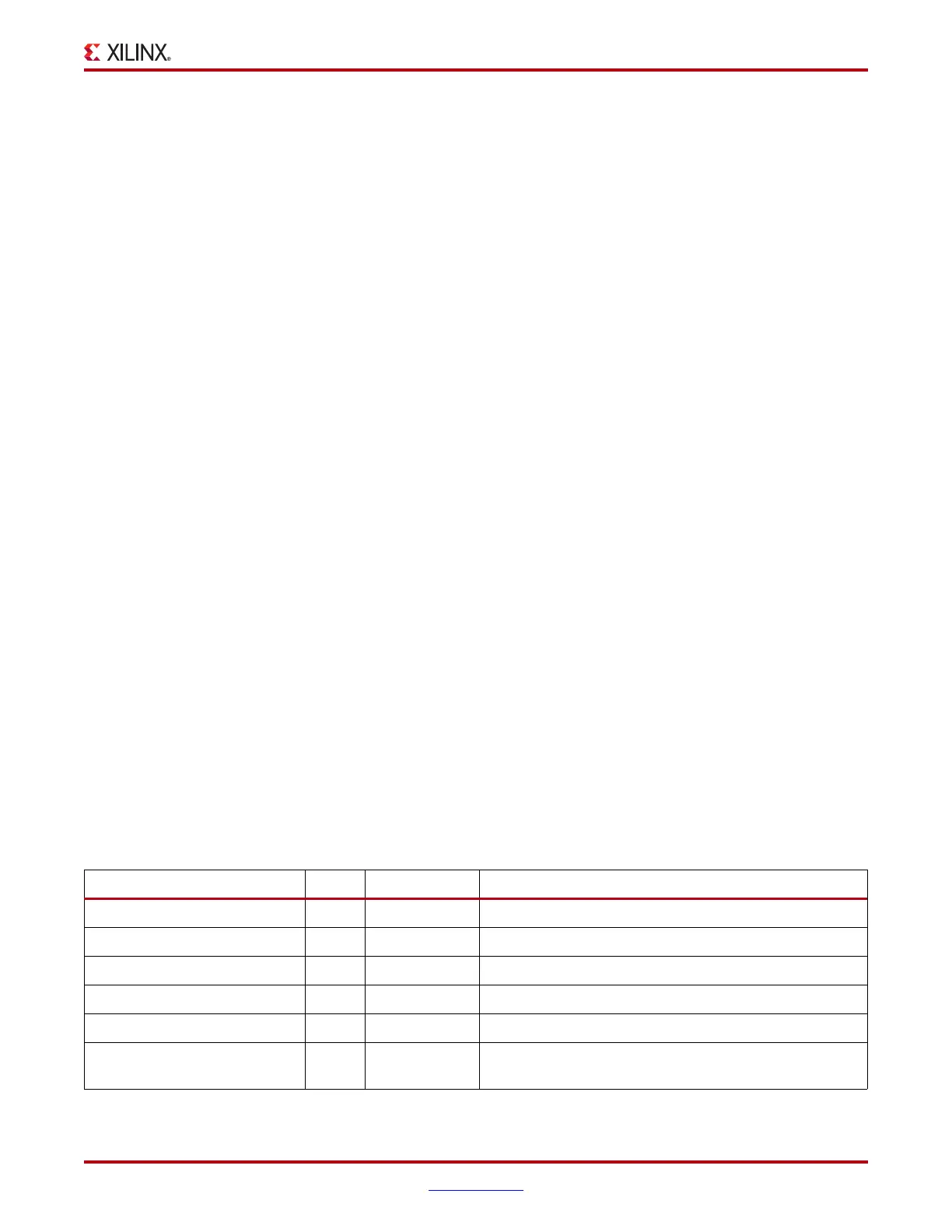
Table 3-18 defines the TX buffer bypass ports.
Table 3-18: TX Buffer Bypass Ports
Port Dir Clock Domain Description
TXDLYALIGNDISABLE In Async Reserved. Must be tied High.
TXDLYALIGNMONENB In Async Reserved. Must be tied High.
TXDLYALIGNMONITOR[7:0] Out Async Reserved.
TXDLYALIGNOVERRIDE In Async Reserved. Must be tied Low.
TXDLYALIGNRESET In Async Reserved. Must be tied High.
TXDLYALIGNUPDSW In Async Reserved. Use recommended values from the Virtex-6
FPGA GTX Transceiver Wizard.

 Loading...

