132 www.xilinx.com Virtex-6 FPGA GTX Transceivers User Guide
UG366 (v2.5) January 17, 2011
Chapter 3: Transmitter
Refer to the Virtex-6 FPGA Data Sheet for the maximum clock frequency and jitter
limitations of BUFR. For details about placement constraints and restrictions on clocking
resources (MMCM, BUFGCTRL, IBUFDS_GTXE1, BUFG, etc.), refer to the Virtex-6 FPGA
Clocking Resources User Guide.
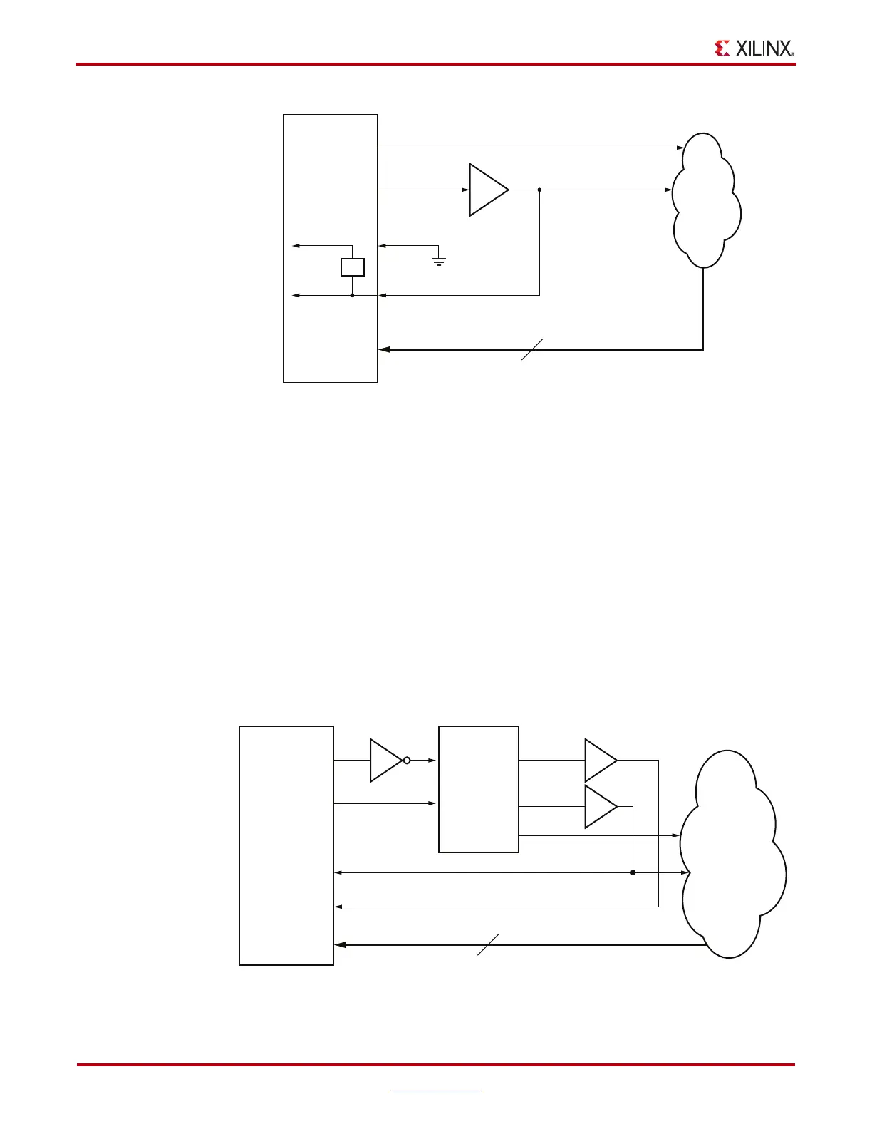
TXOUTCLK Driving a GTX TX in 4-Byte Mode (Single Lane)
Figure 3-3 uses 4-byte wide datapaths (TX_DATA_WIDTH = 32 or 40). TXOUTCLK is
used to drive the CLKIN of the MMCM to derive two positive-edge aligned CLKOUT0
and CLKOUT1 signals, where the CLKOUT1 frequency is equal to the CLKOUT0
frequency divided by 2. If the TX PLL is not used and is derived from the RX PLL, the
active-High RXPLLLKDET signal should be used to deassert the RST signal of the MMCM.
TXOUTCLK can be used to drive CLKIN directly without using the BUFG resources. In the
use models where TX Buffer is bypassed, TXOUTCLK must drive CLKIN directly. This
requires the MMCM to be placed in the same clock region as the driving GTX.
X-Ref Target - Figure 3-2
Figure 3-2: TXOUTCLK Drives TXUSRCLK2 (2-Byte Mode)
GTX
Transceiver
TXPLLLKDET/
RXPLLLKDET
TXUSRCLK
Design
in
FPGA
TXUSRCLK2
TXUSRCLK
TXOUTCLK
BUFG or
BUFR
/1
TXUSRCLK2
TXDATA (16 or 20 bits)
UG366_c3_23_061609
X-Ref Target - Figure 3-3
Figure 3-3: MMCM Provides Clocks for 4-Byte Wide Datapath
GTX
Transceiver
TXPLLLKDET/
RXPLLLKDET
Design
in
FPGA
TXUSRCLK2
(1)
TXOUTCLK
RST
CLKIN
CLKOUT0
CLKOUT1
BUFG or
BUFR
LOCKED
TXUSRCLK
(1)
MMCM
T XDATA (32 or 40 bits)
Note 1: F
TXUSRCLK2
= F
TXUSRCLK
/2
UG366_c3_25_061609

 Loading...

