Virtex-6 FPGA GTX Transceivers User Guide www.xilinx.com 161
UG366 (v2.5) January 17, 2011
TX Buffer Bypass
For phase alignment to be effective, TXUSRCLK and TXUSRCLK2 for all GTX transceivers
must come from the same source and must be routed through a low-skew clocking
resource (such as BUFG,BUFR or MMCM). When TXOUTCLK is used as the clock source
in TX buffer bypass mode, TXOUTCLK_CTRL must select either TXPLLREFCLK_DIV1 or
TXPLLREFCLK_DIV2. Refer to Figure 3-5, page 134, Figure 3-6, page 135, and Figure 3-7,
page 136 for additional examples on how TXUSRCLK and TXUSRCLK2 signals should be
driven for low-skew operation.
Transmit Fabric Clocking Use Model for TX Buffer Bypass
The system margin in TX Buffer Bypass mode depends on the following:
• TXUSRCLK frequency (See Equation 3-1)
• Clocking resources used to generate TXUSRCLK from TXOUTCLK (BUFG, BUFR or
MMCM)
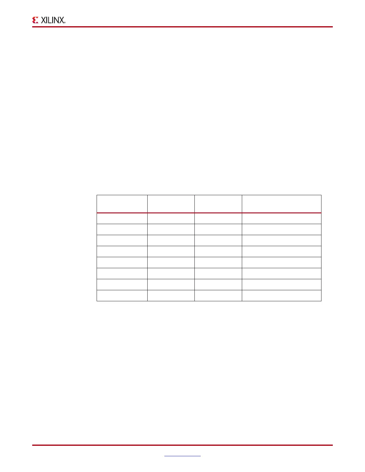
Table 3-21 describes the required clocking use model when bypassing the TX Buffer as a
function of the line rate and the internal Data Width. To enhance the system margin for
better compensation to Temperature and/or Voltage drift, these requirements must be met.
FPGA TX Interface describes these clocking use models in detail. Figures Figure 3-2 and
Figure 3-5 describe the clocking use model with BUFG and BUFR. Figures Figure 3-3 and
Figure 3-6 describe the clocking use model with MMCM.
Table 3-21: Required Clocking Use Model When bypassing the TX Buffer as a
Function of the Line Rate and the internal Data Width
Line Rate (Gb/s)
Internal Data
Width
Device Clocking Use Model
4.2 20-bit 240T BUFG, BUFR, MMCM
(1)
5.8 20-bit 240T BUFR, MMCM
(1)
6.2 20-bit 240T MMCM
(1)
6.6 20-bit 240T MMCM
(1)
4.2 16-bit 240T BUFG, BUFR, MMCM
(1)
4.6 16-bit 240T BUFR, MMCM
(1)
4.9 16-bit 240T MMCM
(1)
6.6 16-bit 240T MMCM
(1)
1. MMCM must be placed in the same clock region as the driving GTX. For details about placement
constraints and restrictions on clocking resources (BUFG, BUFR, MMCM, etc.), refer to the Virtex-
6 FPGA Clocking Resources User Guide.

 Loading...

