Virtex-6 FPGA GTX Transceivers User Guide www.xilinx.com 101
UG366 (v2.5) January 17, 2011
Chapter 2
Shared Transceiver Features
Reference Clock Input Structure
Functional Description
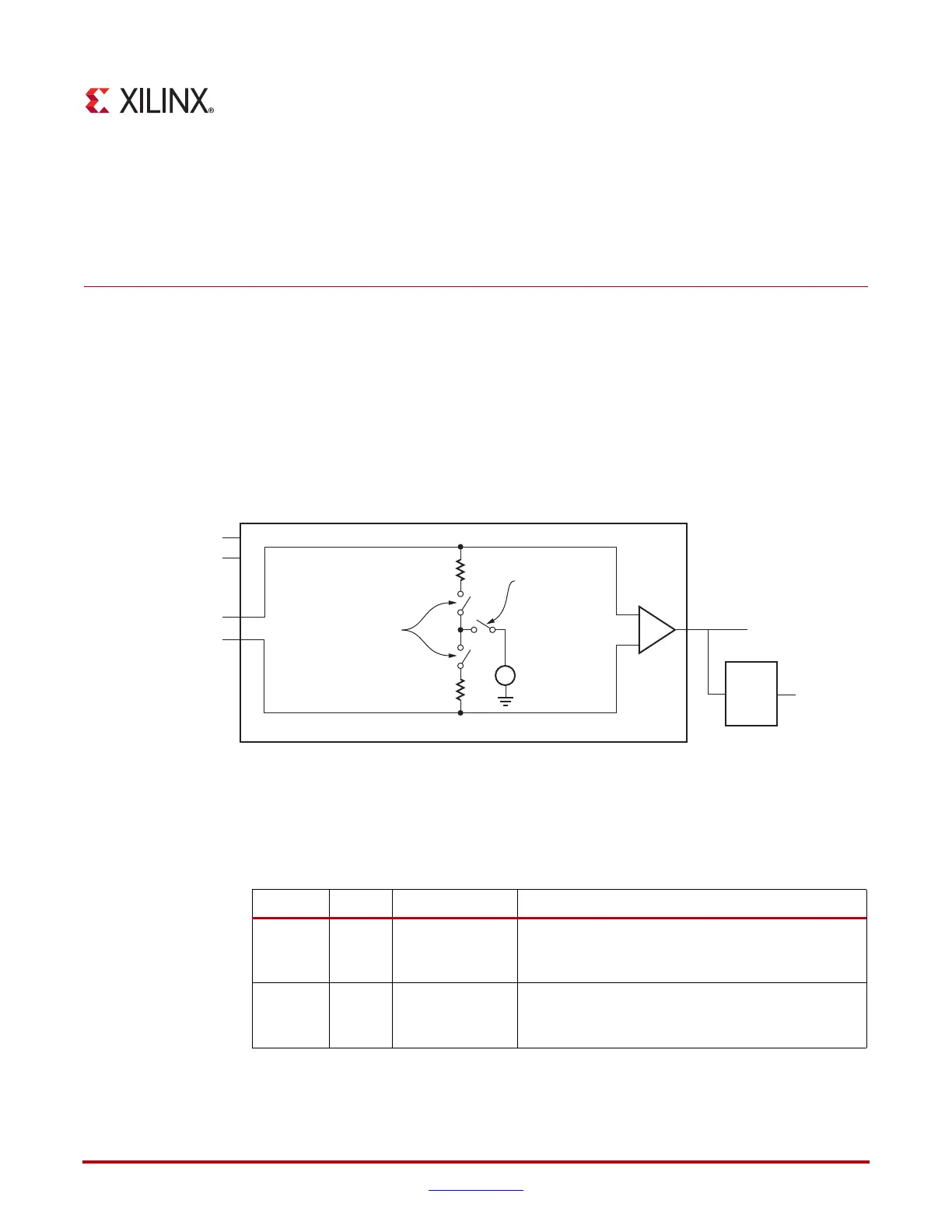
The reference clock input structure is illustrated in Figure 2-1. The input is terminated
internally with 50 on each leg to 4/5MGTAVCC. The reference clock is instantiated in
software with the IBUFDS_GTXE1 software primitive. The ports and attributes controlling
the reference clock input are tied to the IBUFDS_GTXE1 software primitive.
Ports and Attributes
Table 2-1 defines the reference clock input ports in the IBUFDS_GTXE1 software primitive.
X-Ref Target - Figure 2-1
Figure 2-1: Reference Clock Input Structure
+
–
UG366_c2_10_110210
Nom
50Ω
CLKRCV_TRST =
MGTREFCLKP0/1
MGTREFCLKN0/1
MGTAVCC = 1.0V
CLKCM_CFG
4/5 MGTAVCC
Nom
50Ω
MGTAVSS
I
IB
/2
O
ODIV2
Table 2-1: Reference Clock Input Ports (IBUFDS_GTXE1)
Port Dir Clock Domain Description
I
IB
In
(Pad)
N/A These are the reference clock input ports that get
mapped to MGTREFCLK0P/MGTREFCLK0N and
MGTREFCLK1P/MGTREFCLK1P.
CEB In N/A This is the active-Low asynchronous clock enable
signal for the clock buffer. Pulling this signal High
powers down the clock buffer.

 Loading...

