314 www.xilinx.com Virtex-6 FPGA GTX Transceivers User Guide
UG366 (v2.5) January 17, 2011
Appendix B: DRP Address Map of the GTX Transceiver
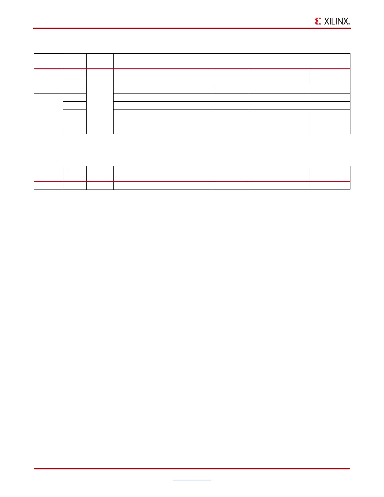
4Ch
15:8
R/W
TX_DLYALIGN_OVRDSETTING 7:0 0-255
1
(1)
7:4 TX_DLYALIGN_LPFINC 3:0 0-15 1
(1)
3:0 TX_DLYALIGN_CTRINC 3:0 0-15 1
(1)
4Dh
15:8 RX_DLYALIGN_OVRDSETTING 7:0 0-255
1
(1)
7:4 RX_DLYALIGN_LPFINC 3:0 0-15 1
(1)
3:0 RX_DLYALIGN_CTRINC 3:0 0-15 1
(1)
4Eh
15:0 R/W Reserved 15:0
4Fh
15:0 R/W Reserved 15:0
Notes:
1. The DRP has the same binary encoding value as the attribute encoding value.
Table B-1: Attributes DRP Address Map (Cont’d)
DADDR
DRP Bits R/W Attribute Name Attribute Bits Attribute Encoding
DRP Binary
Encoding
Table B-2: Status Registers DRP Address Map
DADDR
DRP Bits R/W Register Name Register Bits
Register Encoding
DRP Binary
Encoding
82h
(2)
15:0 R
RX_PRBS_ERR_CNT
15:0
0-65535
1
(1)
Notes:
1. The DRP has the same binary encoding value as the attribute encoding value.
2. The receiver has to be operational for this DRP register to take effect.

 Loading...

