Virtex-6 FPGA GTX Transceivers User Guide www.xilinx.com 281
UG366 (v2.5) January 17, 2011
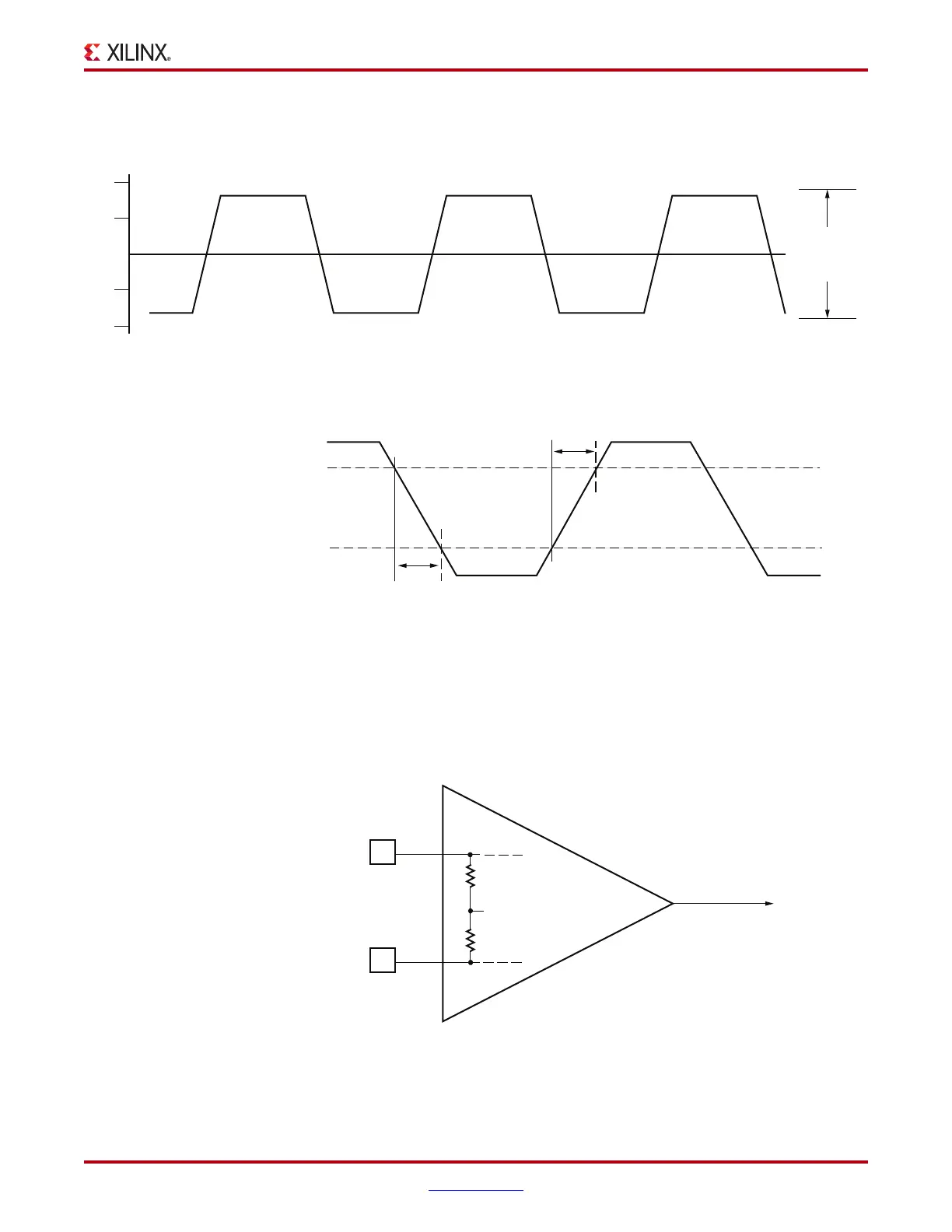
Reference Clock
Figure 5-6 illustrates the differential clock input voltage swing, peak-to-peak, which is
defined as MGTREFCLKP – MGTREFCLKN.
Figure 5-7 shows the rise and fall time convention of the reference clock.
Figure 5-8 illustrates the internal details of the IBUFDS. The dedicated differential
reference clock input pair MGTREFCLKP/MGTREFCLKN is internally terminated with
100 differential impedance. The common mode voltage of this differential reference clock
input pair is 4/5 of MGTAVCC, or nominal 0.8V. MGTAVCC is nominally 1.0V, hence the
common mode voltage is nominally 800 mV. The resistor values given in Figure 5-8 are
nominal. Refer to the Virtex-6 FPGA Data Sheet for exact specifications.
X-Ref Target - Figure 5-6
Figure 5-6: Differential Clock Input Voltage Swing, Peak-to-Peak
UG366_c5_06_051509
0
+V
–V
MGTREFCLKP - MGTREFCLKN
V
IDIFF
X-Ref Target - Figure 5-7
Figure 5-7: Rise and Fall Times
X-Ref Target - Figure 5-8
Figure 5-8: MGTREFCLK Input Details
UG366_c5_07_051509
80%
20%
T
FCLK
T
RCLK
UG366_c5_08_051809
REFCLK
MGTREFCLKP
MGTREFCLKN
4/5 MGTAVCC
to GTX
Dedicated
Clock
Routing
50Ω
50Ω

 Loading...

