Virtex-6 FPGA GTX Transceivers User Guide www.xilinx.com 193
UG366 (v2.5) January 17, 2011
RX Out-of-Band Signaling
Table 4-10 defines the RX OOB attributes.
RXSTATUS[2:0] Out RXUSRCLK2 RXSTATUS[2:0] are used only for PCIe mode, as defined by the
PIPE specification.
RXVALID Out RXUSRCLK2 Indicates symbol lock and valid data on RXDATA and
RXCHARISK[3:0] when High, as defined in the PIPE
specification.
Table 4-9: RX OOB Ports
Port Direction Clock Domain Description
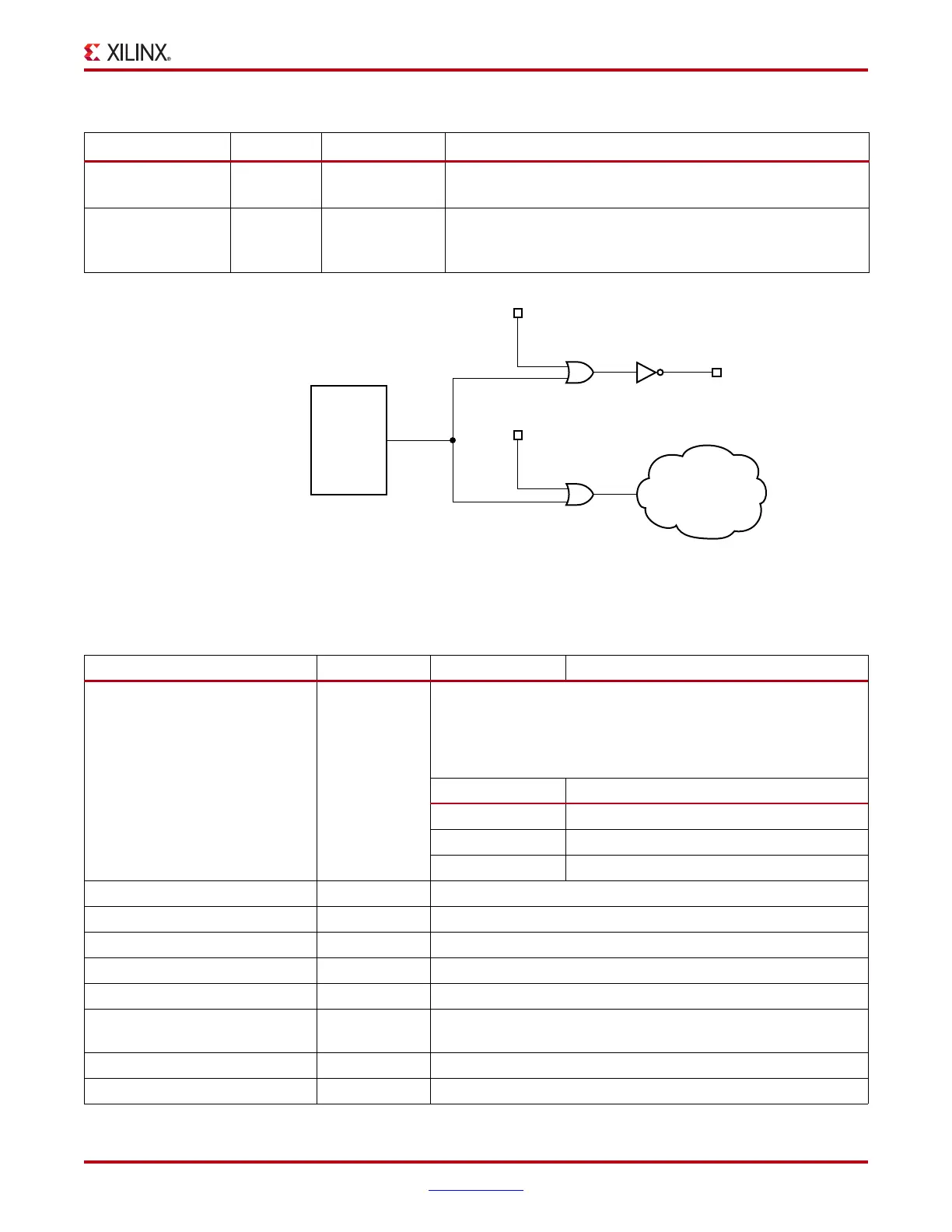
X-Ref Target - Figure 4-8
Figure 4-8: Optional Ports GATERXELECIDLE and IGNORESIGDET
PMA
(RX Signal
Detection
Logic)
GTX
Transceivers
Logic
GATERXELECIDLE
IGNORESIGDET
RXELECIDLE
UG366_c4_49_072309
Table 4-10: RX OOB Attributes
Attribute Type Description
OOBDETECT_THRESHOLD 3-bit Binary Sets the minimum differential voltage between RXN and RXP.
When the differential voltage drops below this level, the incoming
signal is considered an OOB signal. This 3-bit binary encoded
attribute has the following nominal values of the OOB threshold
voltage
(1)
:
Value OOB Nominal Threshold Voltage (mV)
000 – 010 Reserved
011 (default) 100
100 – 111 Reserved
SAS_MAX_COMSAS 6-bit Hex Upper bound on the idle count during COMSAS for SAS
SAS_MIN_COMSAS 6-bit Hex Lower bound on the idle count during COMSAS for SAS
SATA_BURST_VAL 3-bit Binary Number of bursts to declare a COM match for SAS/SATA
SATA_IDLE_VAL 3-bit Binary Number of idles to declare a COM match for SAS/SATA
SATA_MAX_BURST 6-bit Hex Upper bound on an activity burst for COM FSM for SAS/SATA
SATA_MAX_INIT 6-bit Hex Upper bound on idle count during COMINIT/COMRESET for
SAS/SATA
SATA_MAX_WAKE 6-bit Hex Upper bound on idle count during COMWAKE for SAS/SATA
SATA_MIN_BURST 6-bit Hex Lower bound on an activity burst for COM FSM for SAS/SATA

 Loading...

