112 www.xilinx.com Virtex-6 FPGA GTX Transceivers User Guide
UG366 (v2.5) January 17, 2011
Chapter 2: Shared Transceiver Features
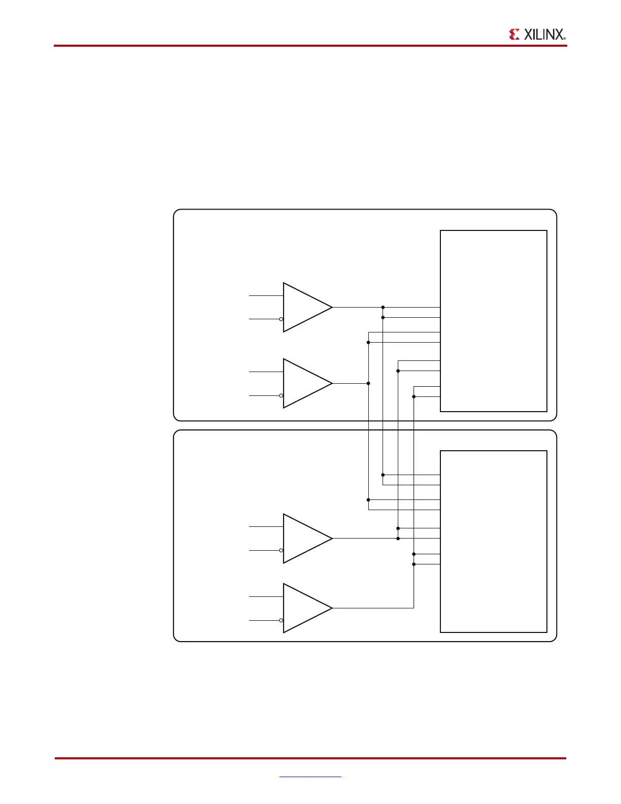
The flexibility of the reference clock selection architecture allows each transceiver within a
Quad to have access to the dedicated reference clocks from the Quad immediately above
and below. Figure 2-7 shows an example of how one of the transceivers belonging to one
quad can access the dedicated reference clocks from another Quad by using the
NORTHREFCLK and SOUTHREFCLK ports. The Xilinx software tools handle the
complexity of the multiplexers and associated routing for designs that require a single
reference clock per GTX transceiver PLL. In situations where there is more than one
reference clock option per GTX transceiver PLL (Figure 2-7), the user design is required to
connect the corresponding ports and set TXPLLREFSELDY[2:0] and
RXPLLREFSELDY[2:0] based on the design requirements.
Note:
The IBUFDS_GTXE1 diagram in Figure 2-6 is a simplification. The output port ODIV2 is left
floating, and the input port CEB is set to logic 0.
X-Ref Target - Figure 2-7
Figure 2-7: Multiple GTX Transceivers with Multiple Reference Clocks in Different
Quads
SOUTHREFCLKTX[0]
SOUTHREFCLKRX[0]
SOUTHREFCLKTX[1]
SOUTHREFCLKRX[1]
NORTHREFCLKTX[0]
NORTHREFCLKRX[0]
NORTHREFCLKTX[1]
NORTHREFCLKRX[1]
MGTREFCLKTX[0]
MGTREFCLKRX[0]
MGTREFCLK0P
MGTREFCLK0N
I
IB
O
MGTREFCLK1P
MGTREFCLK1N
UG366_c2_09_061409
I
IB
O
MGTREFCLKTX[1]
MGTREFCLKRX[1]
GTXE1
Q
(n)
IBUFDS_GTXE1
IBUFDS_GTXE1
SOUTHREFCLKTX[0]
SOUTHREFCLKRX[0]
SOUTHREFCLKTX[1]
SOUTHREFCLKRX[1]
NORTHREFCLKTX[0]
NORTHREFCLKRX[0]
NORTHREFCLKTX[1]
NORTHREFCLKRX[1]
MGTREFCLKTX[0]
MGTREFCLKRX[0]
MGTREFCLK0P
MGTREFCLK0N
I
IB
O
MGTREFCLK1P
MGTREFCLK1N
I
IB
O
MGTREFCLKTX[1]
MGTREFCLKRX[1]
GTXE1
Q
(n+1)
IBUFDS_GTXE1
IBUFDS_GTXE1

 Loading...

