Virtex-6 FPGA GTX Transceivers User Guide www.xilinx.com 111
UG366 (v2.5) January 17, 2011
Reference Clock Selection
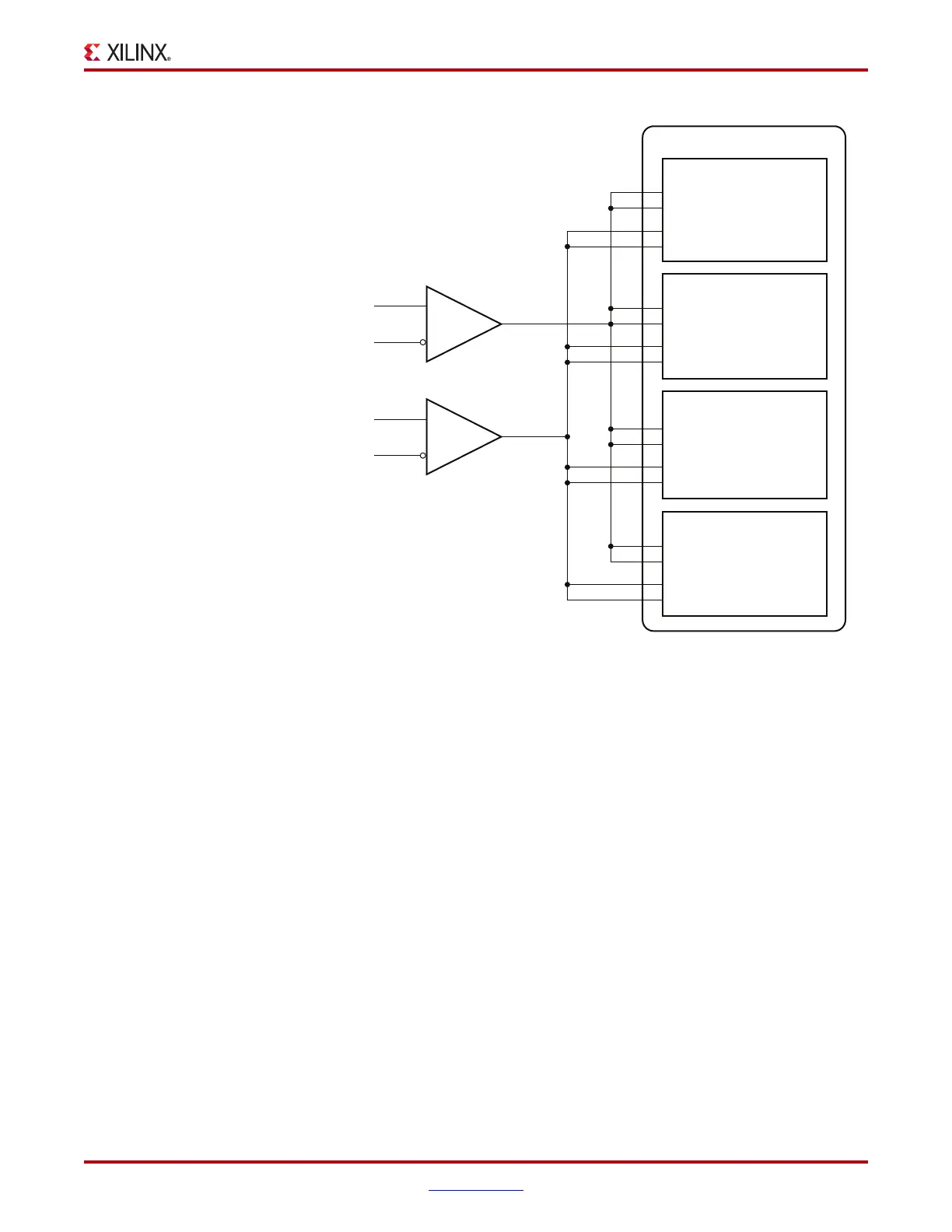
Note: The IBUFDS_GTXE1 diagram in Figure 2-6 is a simplification. The output port ODIV2 is left
floating, and the input port CEB is set to logic 0.
The User Constraints File (UCF) can be used to constrain the location of the transceivers
and the corresponding reference clock source location. For example, if Q(n) in Figure 2-6
belongs to QUAD_114 of an LX75T-FF484 device (as shown in Figure 1-6, page 43), these
constraints can be applied:
## Set placement for the corresponding GTXE1 instances
INST rocketio_wrapper_i/gtx0_rocketio_wrapper_i/gtxe1_i LOC=GTXE1_X0Y0;
INST rocketio_wrapper_i/gtx1_rocketio_wrapper_i/gtxe1_i LOC=GTXE1_X0Y1;
INST rocketio_wrapper_i/gtx2_rocketio_wrapper_i/gtxe1_i LOC=GTXE1_X0Y2;
INST rocketio_wrapper_i/gtx3_rocketio_wrapper_i/gtxe1_i LOC=GTXE1_X0Y3;
## Reference clock constraints. Assign the IBUFDS_GTXE1 input nets to the
## package pins for the corresponding dedicated clock sources
## MGTREFCLK0[P/N]_114 or MGTREFCLK1[P/N]_114.
NET MGTREFCLK0N LOC=U3;
NET MGTREFCLK0P LOC=U4;
NET MGTREFCLK1N LOC=R3;
NET MGTREFCLK1N LOC=R4;
Figure 2-6 shows that the TX PLL and RX PLL of each transceiver can be sourced by either
MGTREFCLK0[P/N] or MGTREFCLK1[P/N]. Users can set TXPLLREFSELDY[2:0] and
RXPLLREFSELDY[2:0] to the corresponding value as shown in Figure 2-3, page 105.
X-Ref Target - Figure 2-6
Figure 2-6: Multiple GTX Transceivers with Multiple Reference Clocks
MGTREFCLKTX[0]
MGTREFCLKRX[0]
MGTREFCLKTX[1]
MGTREFCLKRX[1]
MGTREFCLKTX[0]
MGTREFCLKRX[0]
MGTREFCLK0P
MGTREFCLK0N
I
IB
O
MGTREFCLK1P
MGTREFCLK1N
UG366_c2_08_081109
I
IB
O
MGTREFCLKTX[1]
MGTREFCLKRX[1]
MGTREFCLKTX[0]
MGTREFCLKRX[0]
MGTREFCLKTX[1]
MGTREFCLKRX[1]
MGTREFCLKTX[0]
MGTREFCLKRX[0]
MGTREFCLKTX[1]
MGTREFCLKRX[1]
GTXE1
GTXE1
GTXE1
GTXE1
Q
(n)
IBUFDS_GTXE1
IBUFDS_GTXE1

 Loading...

