Virtex-6 FPGA GTX Transceivers User Guide www.xilinx.com 105
UG366 (v2.5) January 17, 2011
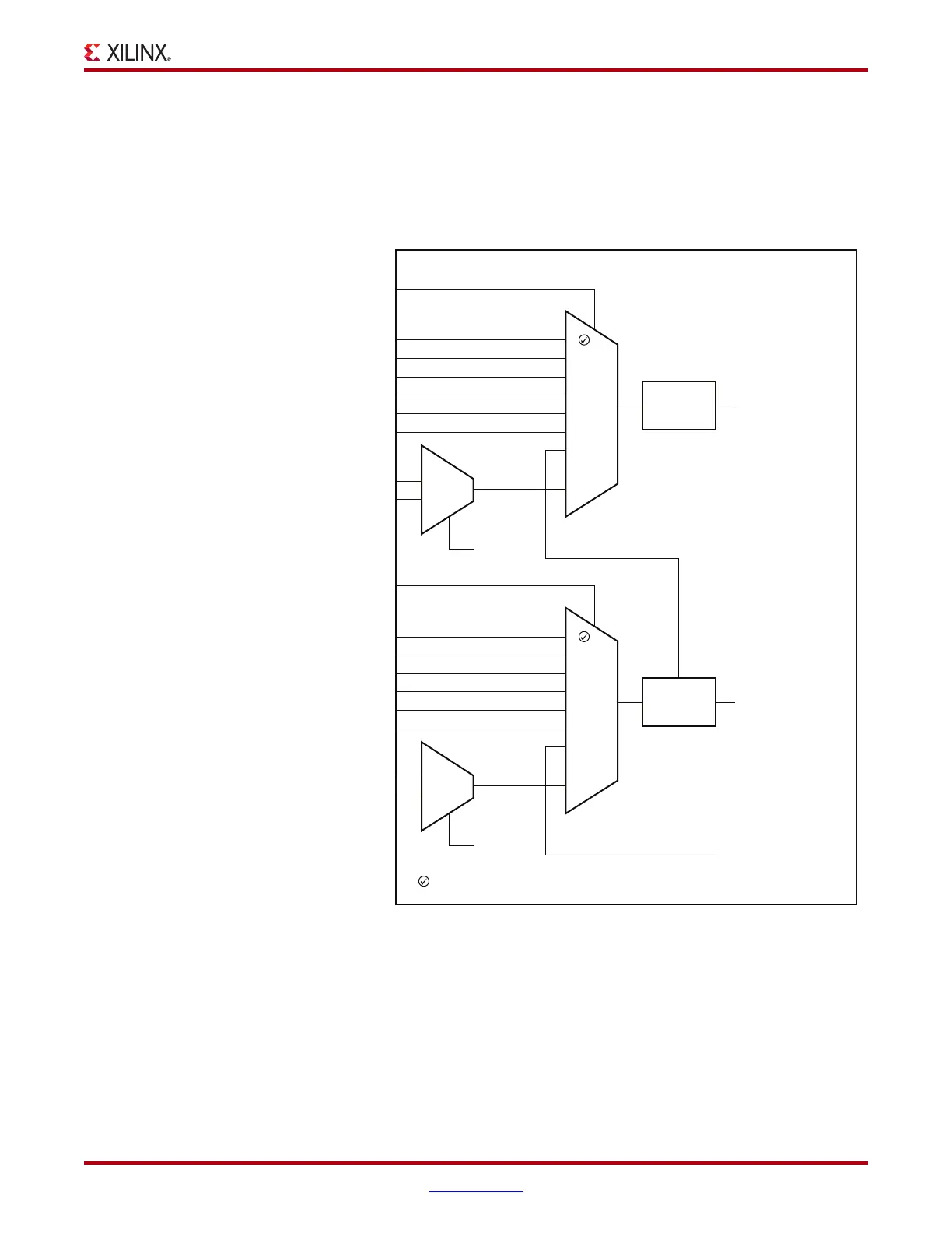
Reference Clock Selection
Figure 2-3 shows the detailed view of the reference clock multiplexer structure within a
single GTXE1 primitive. The TXPLLREFSELDY and RXPLLREFSELDY ports are required
when multiple reference clocks are used. A single reference clock is most commonly used.
In this case, the TXPLLREFSELDY and RXPLLREFSELDY ports can be connected to 000,
and the Xilinx software tools handle the complexity of the multiplexers and associated
routing. See Single External Reference Clock Use Model for more information.
The four GTX transceivers that make up a Quad share two dedicated reference clock pin
pairs. The user design accesses these reference clocks by instantiating IBUFDS_GTXE1
primitives. These reference clocks can be used locally by any of the four GTX transceivers
X-Ref Target - Figure 2-3
Figure 2-3: GTX Transceiver Detailed Diagram
MGTREFCLKTX[0]
MGTREFCLKTX[1]
NORTHREFCLKTX[0]
NORTHREFCLKTX[1]
SOUTHREFCLKTX[0]
SOUTHREFCLKTX[1]
GREFCLKTX
PERFCLKTX
TXPLLREFSELDY[2:0]
0
1
2
3
4
5
6
7
Out
TX PLL
TX PLL REFCLK
0
1
Out
CORECLK
CAS_CLK
GTX Transceiver
See
Note 1
MGTREFCLKRX[0]
MGTREFCLKRX[1]
NORTHREFCLKRX[0]
NORTHREFCLKRX[1]
SOUTHREFCLKRX[0]
SOUTHREFCLKRX[1]
GREFCLKRX
PERFCLKRX
RXPLLREFSELDY[2:0]
0
1
2
3
4
5
6
7
Out
RX PLL
RX PLL REFCLK
0
1
Out
CORECLK
NC
(2)
See
Note 1
Default Configuration
UG366_c2_02_051509
Notes:
1. The CORECLK multiplexer is controlled by software. If GREFCLK is connected, software configures
the multiplexer to use GREFCLK. If the PERFCLK is connected, software configures the multiplexer
to use PERFCLK. There is no user-controllable attribute to switch the multiplexer. Only one of the
inputs can be connected at a time.
2. The CAS_CLK input to the RX PLL is not used or configured.

 Loading...

