3–12 Altera Corporation
Stratix Device Handbook, Volume 2 June 2006
DDR Memory Support Overview
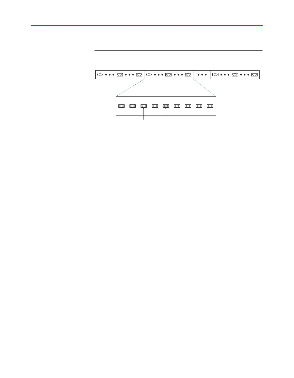
Figure 3–7 shows the DQ and DQS pins in ×8 mode.
Figure 3–7. Stratix & Stratix GX Device DQ & DQS Groups in × 8 Mode
Note to Figure 3–7:
(1) There are at least eight DQ pins per group.
Data & Data Strobe Pins
Stratix and Stratix GX data pins for the DDR memory interfaces are called
DQ pins. The Stratix and Stratix GX device I/O banks at the top (I/O
banks 3 and 4) and the bottom (I/O banks 7 and 8) of the device support
DDR SDRAM and RLDRAM II up to 200 MHz. These pins support DQS
signals with DQ bus modes of ×8, ×16, or ×32. Stratix and Stratix GX
devices can support either bidirectional data strobes or uni-directional
read clocks. Depending on the external memory interface, either the
memory device's read data strobes or read clocks feed the DQS pins.
For ×8 mode, there are up to 20 groups of programmable DQS and DQ
pins—10 groups in I/O banks 3 and 4 and 10 groups in I/O banks 7 and 8
(see Table 3–3). Each group consists of one DQS pin and a set of eight DQ
pins.
For ×16 mode, there are up to eight groups of programmable DQS and
DQ pins—four groups in I/O banks 3 and 4, and four groups in I/O
banks 7 and 8. The EP1S20 device supports seven ×16 mode groups. The
EP1S10 device does not support ×16 mode. All other devices support the
full eight groups. See Table 3–3. Each group consists of one DQS and 16
DQ pins. In ×16 mode, DQS1T, DQS3T, DQS6T, and DQS8T pins on the top
side of the device, and DQS1B, DQS3B, DQS6B, and DQS8B pins on the
DQ Pins
1
DQS Pin
Top or Bottom I/O Bank