Altera Corporation 3–21
June 2006 Stratix Device Handbook, Volume 2
External Memory Interfaces in Stratix & Stratix GX Devices
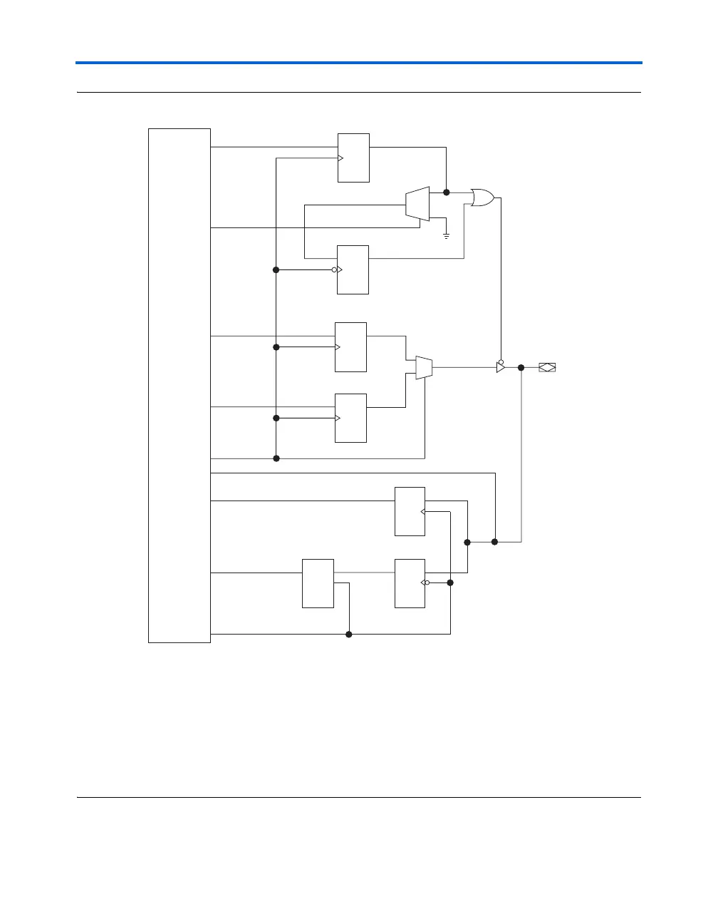
Figure 3–10. Bidirectional DDR I/O Path in Stratix & Stratix GX Devices Note (1)
Notes to Figure 3–10:
(1) All control signals can be inverted at the IOE. No programmable delay chains are shown in this diagram.
(2) The OE signal is active low, but the Quartus II software implements this as active high and automatically adds an
inverter before input to the A
OE
register during compilation.
(3) The A
OE
register generates the enable signal for general-purpose DDR I/O applications.
(4) This select line is to choose whether the OE signal should be delayed by half-a-clock cycle.
(5) The B
OE
register generates the delayed enable signal for the write strobes and write clock for memory interfaces.
(6) The tristate enable is active low by default. You can design it to be active high. The combinational control path for
the tristate is not shown in this diagram.
(7) You can also have combinational output to the I/O pin; this path is not shown in the diagram.
DQ
DFF
DQ
ENA
DQ
DFF
Input Register B
I
Input Register A
I
Latch C
DQ
DFF
DQ
DFF
0
1
Output Register A
O
Output Register B
O
DQ
DFF
DQ
DFF
OR2
TRI
I/O Pin (7)
OE Register B
OE
OE Register A
OE
Logic Array
dataout_l
dataout_h
outclock
datain_h
datain_l
OE
inclock
neg_reg_out
I
0
(5)
(4)
(6)
(3)
combout
1
(2)
Latch
TCHLA