3–22 Altera Corporation
Stratix Device Handbook, Volume 2 June 2006
DDR Memory Support Overview
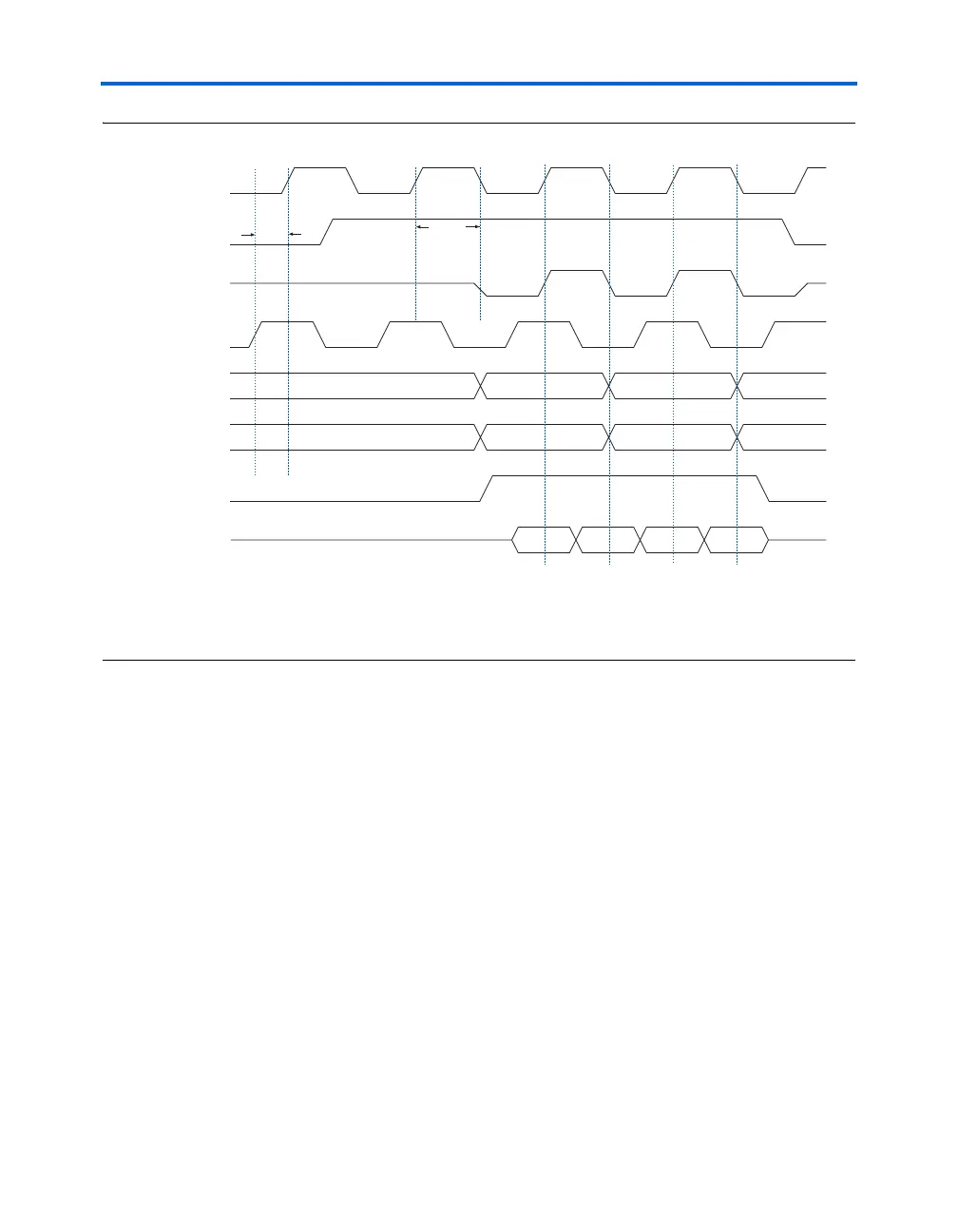
Figure 3–11. Extending the OE Disable by Half-a-Clock Cycle for a Write Transaction Note (1)
Note to Figure 3–11:
(1) The waveform reflects the software simulation result. The OE signal is an active low on the device. However, the
Quartus II software implements this signal as an active high and automatically adds an inverter before the A
OE
register D input.
Figures 3–12 and 3–13 summarize the IOE registers used for the DQ and
DQS signals.
D0
D0 D2
D1
D1 D3
D2 D3
Preamble
Postamble
System clock
(outclock for DQS)
OE for DQS
(from logic array)
datain_h
(from logic array)
datain_l
(from logic array)
OE for DQ
(from logic array)
Write Clock
(outclock for DQ,
−90° phase shifted
from System Clock)
DQS
DQ
Delay
by Half
a Clock
Cycle
90˚