5–26 Altera Corporation
Stratix Device Handbook, Volume 2 July 2005
Receiver Data Realignment
RXLOADEN signal and dropping the first incoming bit of the serial input
data stream located in the first serial register of the SERDES circuitry
(shown in Figure 5–3 on page 5–8).
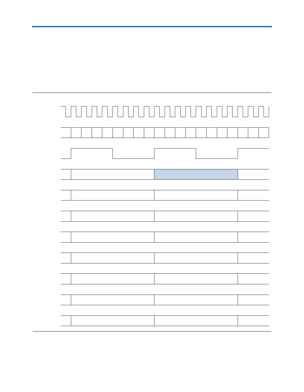
Figure 5–18 shows the function-timing diagram of a Stratix SERDES in
normal
×8 mode, and Figure 5–19 shows the function-timing diagrams of
a Stratix SERDES when data realignment is used.
Figure 5–18. SERDES Function Timing Diagram in Normal Operation
×8 clock
×1 clock
D7 D0 D1 D2
D2 D2 D2
D3 D4 D5 D6 D7 D0 D1 D2 D7 D0 D1 D2D3 D4 D5 D6
D3 D3 D3
D4 D4 D4
D5 D5 D5
D6 D6 D6
D7 D7 D7
D0 D0 D0
D1
PD7
Serial data
PD6
PD5
PD4
PD3
PD2
PD1
PD0 D1 D1