Altera Corporation 5–35
July 2005 Stratix Device Handbook, Volume 2
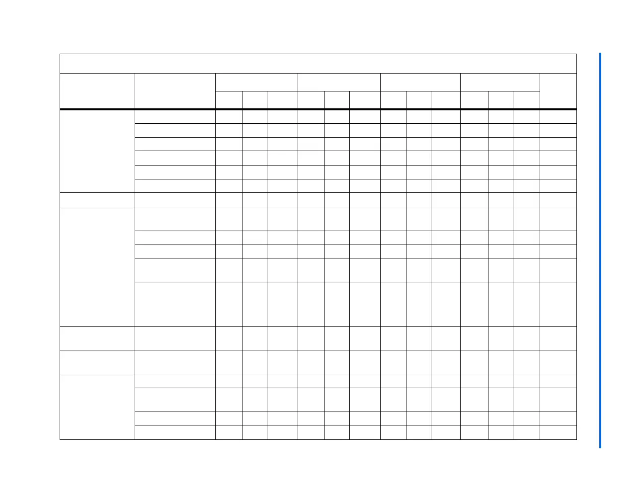
Source-Synchronous Timing Budget
f
HSDR
Device
operation (PCML)
J = 10 300 400 300 400 300 311 300 311 Mbps
J = 8 300 400 300 400 300 311 300 311 Mbps
J = 7 300 400 300 400 300 311 300 311 Mbps
J = 4 300 400 300 400 300 311 300 311 Mbps
J = 2 100 400 100 400 100 300 100 300 Mbps
J = 1 100 250 100 250 100 200 100 200 Mbps
TCCS All 200 200 300 300 ps
SW PCML (J = 4, 7, 8,
10)
750 750 800 800 ps
PCML (J = 2) 900 900 1,200 1,200 ps
PCML (J = 1) 1,500 1,500 1,700 1,700 ps
LVDS and LVPECL
(J =1)
500 500 550 550 ps
LVDS, LVPEC L,
HyperTransport
technology (J =2
through 10)
440 440 500 500 ps
Input jitter tolerance
(peak-to-peak)
All 250 250 250 250 ps
Output jitter (peak-
to-peak)
All 160 160 200 200 ps
Output t
RISE
LVDS 80 110 120 80 110 120 80 110 120 80 110 120 ps
HyperTransport
technology
110 170 200 110 170 200 120 170 200 120 170 200 ps
LVPECL 90 130 150 90 130 150 100 135 150 100 135 150 ps
PCML 80 110 135 80 110 135 80 110 135 80 110 135 ps
Table 5–7. High-Speed I/O Specifications for Flip-Chip Packages (Part 2 of 3) Notes (1), (2)
Symbol Conditions
-5 Speed Grade -6 Speed Grade -7 Speed Grade -8 Speed Grade
Unit
Min Typ Max Min Typ Max Min Typ Max Min Typ Max