Altera Corporation 5–34
July 2005 Stratix Device Handbook, Volume 2
Source-Synchronous Timing Budget
Tables 5–7 and 5–8 show the high-speed I/O timing for Stratix devices
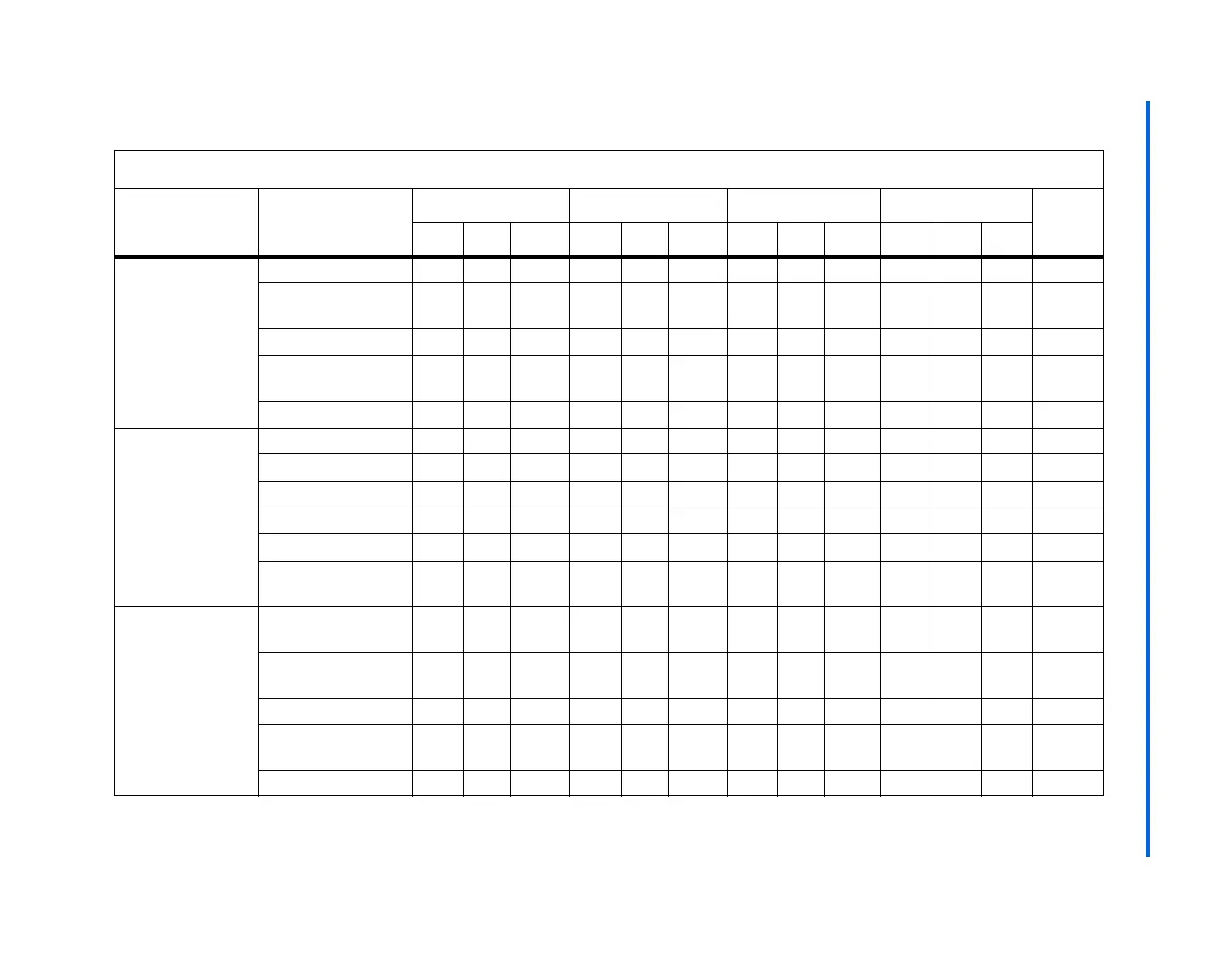
Table 5–7. High-Speed I/O Specifications for Flip-Chip Packages (Part 1 of 3) Notes (1), (2)
Symbol Conditions
-5 Speed Grade -6 Speed Grade -7 Speed Grade -8 Speed Grade
Unit
Min Typ Max Min Typ Max Min Typ Max Min Typ Max
f
HSCLK
(Clock
frequency)
(LVDS, LVPECL,
HyperTransport
technology)
f
HSCLK
= f
HSDR
/ W
W = 4 to 30 10 210 10 210 10 156 10 115.5 MHz
W = 2 (Serdes
bypass)
50 231 50 231 50 231 50 231 MHz
W = 2 (Serdes used) 150 420 150 420 150 312 150 231 MHz
W = 1 (Serdes
bypass)
100 462 100 462 100 462 100 462 MHz
W = 1 (Serdes used) 300 717 300 717 300 624 300 462 MHz
f
HSDR
Device
operation
(LVDS, LVPECL,
HyperTransport
technology)
J = 10 300 840 300 840 300 640 300 462 Mbps
J = 8 300 840 300 840 300 640 300 462 Mbps
J = 7 300 840 300 840 300 640 300 462 Mbps
J = 4 300 840 300 840 300 640 300 462 Mbps
J = 2 100 462 100 462 100 640 100 462 Mbps
J = 1 (LVDS and
LVPECL only)
100 462 100 462 100 640 100 462 Mbps
f
HSCLK
(Clock
frequency)
(PCML)
f
HSCLK
= f
HSDR
/ W
W = 4 to 30 (Serdes
used)
10 100 10 100 10 77.75 10 77.75 MHz
W = 2 (Serdes
bypass)
50 200 50 200 50 150 50 150 MHz
W = 2 (Serdes used) 150 200 150 200 150 155.5 150 155.5 MHz
W = 1 (Serdes
bypass)
100 250 100 250 100 200 100 200 MHz
W = 1 (Serdes used) 300 400 300 400 300 311 300 311 MHz