5–74 Altera Corporation
Stratix Device Handbook, Volume 2 July 2005
Software Support
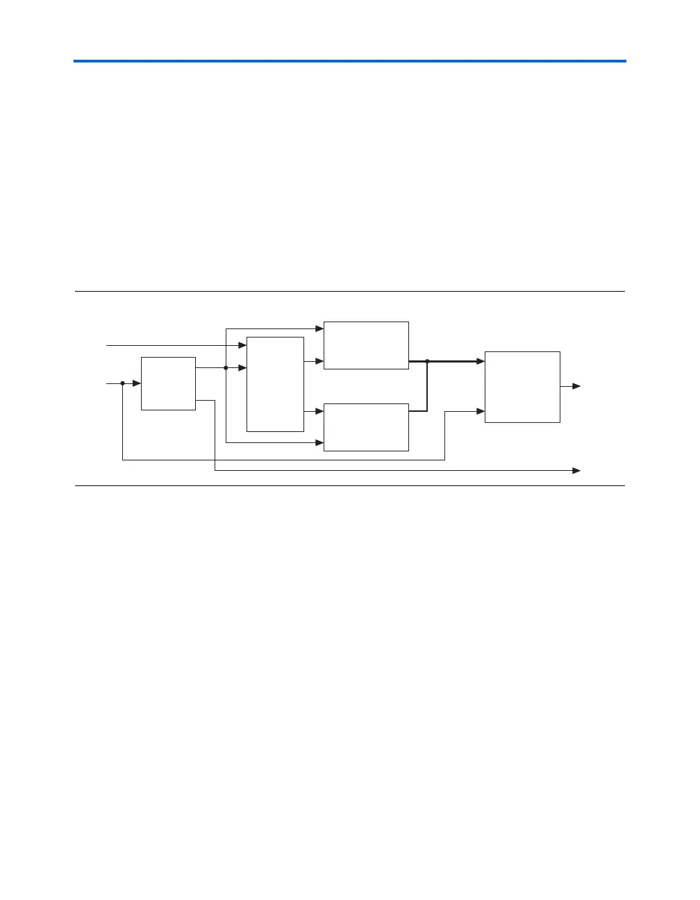
Logic Array as Serializer/Deserializer Interface
The design can use the lpm_shift_reg megafunction instead of a
simple dual port memory block to serialize/deserialize data. The receiver
requires an extra flip-flop clocked by the slow clock to latch on to the
deserialized data. The transmitter requires a counter to generate the
enable signal for the shift register to indicate the times to load and
serialize the data. Figures 5–47 and 5–48 show the schematic of the
×8
LVDS receiver and
×8 LVDS transmitter, respectively, with the logic
array performing the deserialization.
This scheme can also be used for APEX II and Mercury device flexible
LVDS solutions.
Figure 5–47. SERDES Bypass LVDS Receiver with Logic Array as Deserializer
PLL
DDR
Input
Shift
Register
Shift
Register
DFF[7..0]
Clock
Serial
data in
÷2 clock1
×4 clock0
data_l
data[0, 2, 4, 6]
data[1, 3, 5, 7]
data_h
clock
clock
data
data
data[7..0]
Data to
logic array
rx_clk
D
Q
CLK