Altera Corporation 7–23
September 2004 Stratix Device Handbook, Volume 2
Implementing High Performance DSP Functions in Stratix & Stratix GX Devices
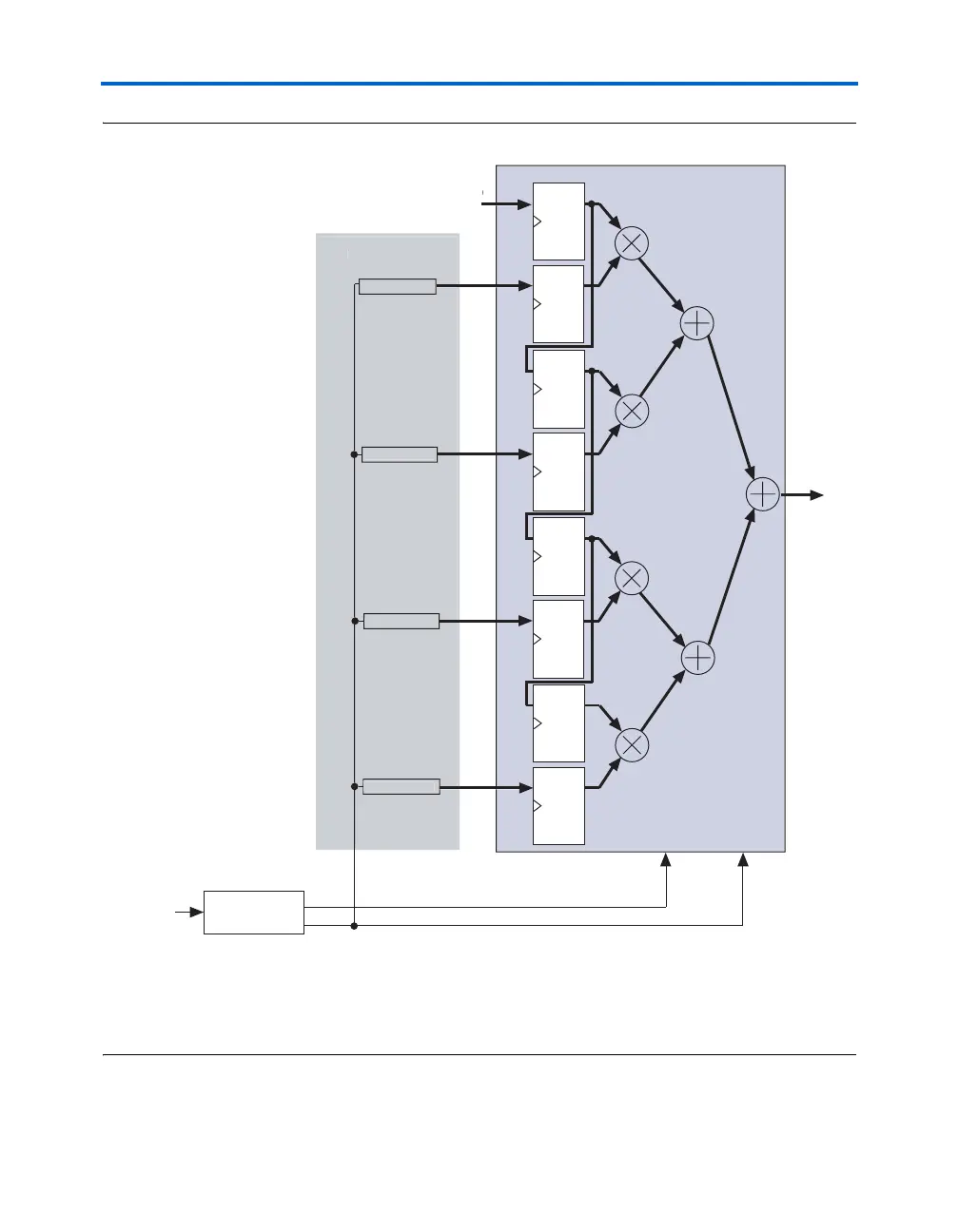
Figure 7–13. Implementation of the Polyphase Interpolation Filter (I=4) Notes (1), (2), (3)
Notes to Figure 7–13:
(1) The 1× clock feeds the input data shiftin register chain.
(2) The 4× clock feeds the input registers for the filter coefficients and other optional registers in the DSP block. See
Note (3).
(3) To increase the DSP block performance, include the pipeline, and output registers. See Figure 7–3 for the details.
0
1
2
3
Filter output
y(n)
Note (2)
Clock input
(1x clock)
1x clock
PLL
DQ
DQ
DQ
DQ
DQ
DQ
DQ
DQ
4x clock
Note (1)
DSP block
Data input
RAM
R
M
RAM
R
M
RAM
R
M
RAM
ROM
Filt
r
o
ffi
i
nt