Altera Corporation 1–13
July 2005 Stratix Device Handbook, Volume 2
General-Purpose PLLs in Stratix & Stratix GX Devices
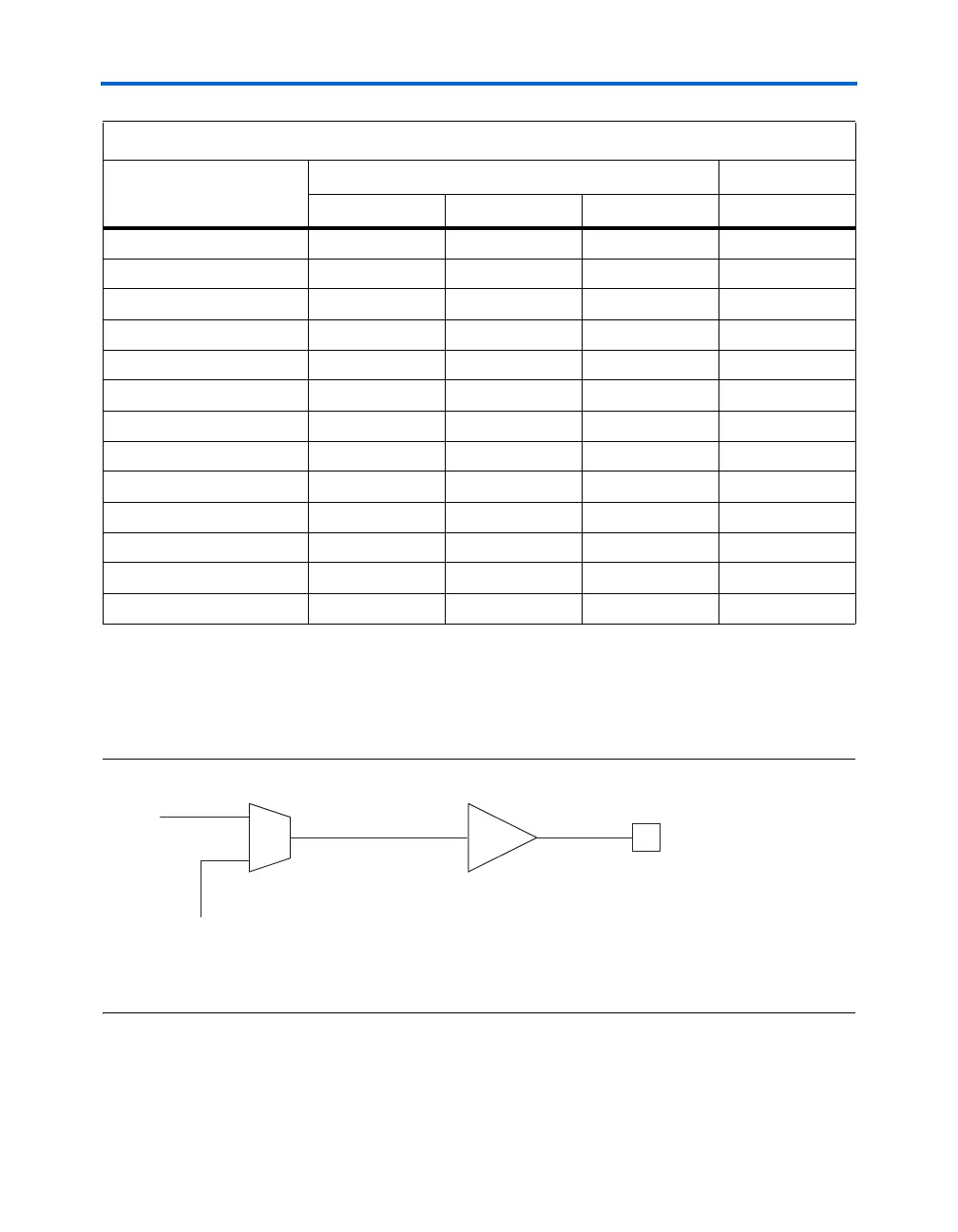
Enhanced PLLs 11 and 12 support one single-ended output each (see
Figure 1–6). These outputs do not have their own VCC and GND signals.
Therefore, to minimize jitter, do not place switching I/O pins next to this
output pin.
Figure 1–6. External Clock Outputs for Enhanced PLLs 11 & 12
Note to Figure 1–6:
(1) For PLL11, this pin is CLK13n; for PLL 12 this pin is CLK6n.
3.3-V GTL+
vv v
1.5-V HSTL Class I
vv v
1.5-V HSTL Class II
vv v
1.8-V HSTL Class I
vv v
1.8-V HSTL Class II
vv v
SSTL-18 Class I
vv v
SSTL-18 Class II
vv v
SSTL-2 Class I
vv v
SSTL-2 Class II
vv v
SSTL-3 Class I
vv v
SSTL-3 Class II
vv v
AGP (1× and 2×)
vv v
CTT
vv v
Table 1–6. I/O Standards Supported for Enhanced PLL Pins (Part 2 of 2)
I/O Standard
Input Output
INCLK FBIN PLLENABLE EXTCLK
CLK13n, I/O, PLL11_OUT
or CLK6n, I/O, PLL12_OUT
(1
From Internal
Logic or IOE
g
0
Counter