1–12 Altera Corporation
Stratix Device Handbook, Volume 2 July 2005
Enhanced PLLs
pair of output pins (four pins total) has dedicated VCC and GND pins to
reduce the output clock’s overall jitter by providing improved isolation
from switching I/O pins.
For PLLs 5 and 6, each pin of a single-ended output pair can either be in
phase or 180° out of phase. The Quartus II software transfers the NOT
gate in the design into the IOE to implement 180° phase with respect to
the other pin in the pair. The clock output pin pairs support the same I/O
standards as standard output pins (in the top and bottom banks) as well
as LVDS, LVPECL, PCML, HyperTransport
TM
technology, differential
HSTL, and differential SSTL. Table 1–6 shows which I/O standards the
enhanced PLL clock pins support. When in single-ended or differential
mode, one power pin supports two differential or four single-ended pins.
Both outputs use the same standards in single-ended mode to maintain
performance. You can also use the external clock output pins as user
output pins if external enhanced PLL clocking is not needed.
The enhanced PLL can also drive out to any regular I/O pin through the
global or regional clock network. The jitter on the output clock is not
guaranteed for this case.
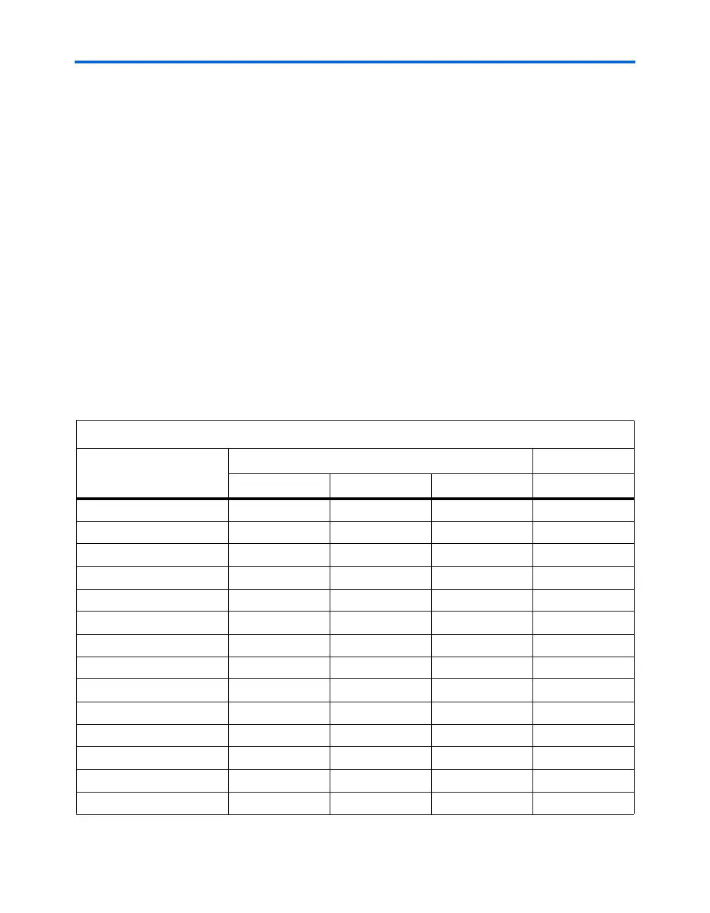
Table 1–6. I/O Standards Supported for Enhanced PLL Pins (Part 1 of 2)
I/O Standard
Input Output
INCLK FBIN PLLENABLE EXTCLK
LVTTL
vvvv
LVCMOS
vvvv
2.5 V
vv v
1.8 V
vv v
1.5 V
vv v
3.3-V PCI
vv v
3.3-V PCI-X 1.0
vv v
LVPECL
vv v
PCML
vv v
LVDS
vv v
HyperTransport technology
vv v
Differential HSTL
vv
Differential SSTL
v
3.3-V GTL
vv v