8–6 Altera Corporation
Stratix Device Handbook, Volume 2 July 2005
Interfaces
Functional Description
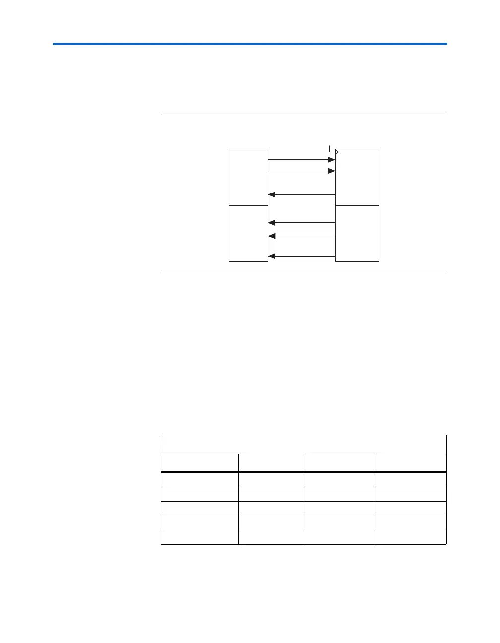
XSBI uses 16-bit LVDS data to interface between the PCS and the PMA
sublayer. Figure 8–4 shows XSBI between these two sublayers.
Figure 8–4. XSBI Functional Block Diagram
On the transmitter side, the transmit data (TX_D[15..0]) is output by
the PCS and input at the PMA using the transmitter clock (PMA_TXCLK),
which is derived from the PMA source clock (PMA_TXCLK_SRC). The
PMA source clock is generated from the PMA with its reference clock
(REFCLK). On the receiver side, the receiver data (RX_D[15..0]) is
output by the PMA and input at the PCS using the PMA-generated
receiver clock (PMA_RXCLK). The SYNC_ERR optional signal is sent to the
PCS by the PMA if the PMA fails to recover the clock from the serial data
stream.
The ratios for these two clocks and data are dependent on the type of PHY
used. Table 8–1 shows the rates for both PHY types.
Table 8–1. XSBI Clock & Data Rates for WAN & LAN PHY
Parameter WAN PHY LAN PHY Unit
TX_D[15..0]
622.08 644.53125 Mbps
PMA_TXCLK
622.08 644.53125 MHz
PMA_TXCLK_SRC
622.08 644.53125 MHz
RX_D[15..0]
622.08 644.53125 Mbps
PMA_RXCLK
622.08 644.53125 MHz
TX_D[15..0]
Transmitter
PMA_TXCLK_SRC
RX_D[15..0]
PMA_RXCLK
Sync_Err (optional)
PMA_TXCLK
REFCLK
PCS
PCS
PMA
PMA
Receiver
Transmitter
Receiver